Request our manufacturing capability
Capabilities
High-Frequency PCB
Introduction to High-Frequency PCB
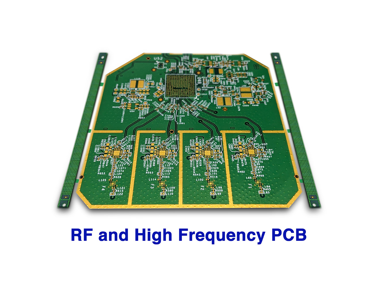
Blind Buried Circuits Inc, manufactures High-frequency PCBs, mainly used for high-speed communications, telecommunications, and RF microwave technology. The purpose of using HF technology (HF PCBs) for communication devices is to offer a fast signal flow and 100 GHz or more frequency range based on the type of material.
Blind Buried Circuits Inc, offers manufacturing of Hi-Speed circuits with most materials containing lower dielectric constant (Dk), lower dissipation factor (Df), and low coefficient of thermal expansion, which transmits electromagnetic waves with minimal losses in signals.

High-Frequency Printed Circuit Board Materials We Offer:
To achieve the optimal performance of high frequency or rf PCB design, our experienced IPC-certified production engineers keep the Hi-Speed Materials in Stock and also suggest alternate materials by considering the purpose of electronic device application, optimal operating frequency signal requirement, and lamination resin loss (etch & fudge) factors based on layer counts requirements in given data stack up.
Regarding the cost & availability of substrate (material), it is well known that Exotic materials like Rogers, Nelco, Megtron, FR408 HR, and Teflon are some of the rare and expensive materials used to fabricate high-frequency PCBs and are not easily available with other manufacturer’s. However, we make all those factors possible for our customers without keeping a hold on manufacturing.
Generally, FR4 substrate doesn’t meet the hi-speed frequencies and can also under the limitations up to 1.6 GHz, due to which FR-4 considerably drops the signal speed. In comparison, Rogers, Nelco, Megtron, and Teflon have low Dk, Df, and water absorption, making them survive in the most challenging environments.
Considering the frequency requirements, we use different substrates and Teflon for frequencies above 10 GHz. Our approved suppliers for high-frequency materials include Arlon, Taconic, Nelco, Isola, Rogers, and Teflon. They all specialize in manufacturing low Dk and Df materials for high-frequency boards.
Do reach out to our team for a hf/rf pcb quote by providing the stack-up requirement
| PCB MATERIAL/SUBSTRATE | ||
|---|---|---|
| RF & Microwaves | ROGERS 4350B, 4003C, 4450F , ROGERS 4835 | |
| OUTER LAYER LINE & SPACING | ||
| STANDARD | ADVANCED | |
| Min. Trace/Space | 2.5mils / 2.5mils | 2mils / 2mils |
| Line Tolerance | +/-15% | +/-8% |
| INNER LAYER | ||
| STANDARD | ADVANCED | |
| Min.Trace/Space | 2mils / 2mils | 1.5mils/1.5mils |
| Line Tolerance | +/-10% | +/-8% |
| BOARD DIMENSIONS | ||
| DESCRIPTION | STANDARD | ADVANCED |
| min. Finish Board Size | 0.2"x0.2" | 0.15"*0.15" |
| Max. Board Thickness | 0.260"(+/-10%) | 0.280"(+/-8%) |
| Min. Board Thickness | 0.007"(+/-10%) | 0.005"(+/-10%) |
| LAMINATION | ||
| DESCRIPTION | STANDARD | ADVANCED |
| Layer Count | 1L to 50L | 60L |
| SURFACE FINISH | ||
| DESCRIPTION | STANDARD | ADVANCED |
| HASL+Selective Hard gold | Yes | Yes |
| Selective ENIG+OSP | Yes | Yes |
| ENIG(Nickel/Gold) | 80-200u"/2-9 u" | 250u"/ 10u" |
| Immersion Silver | 6-18u" | 6-18u" |
| Hard Gold for Tab | 10-80u" | 10-80u" |
| Immersion Tin | 30u"min. | 30u" min. |
| ENEPIG (Ni/Pd/Au) | 125u"/4u"/1u" min. | 150u"/8u"/2u" min. |
| Soft Gold (Nickel/ Gold) | 200u"/ 20u"min. | 200u"/ 20u" |
| SOLDER MASK / RESIST | ||
| DESCRIPTION | STANDARD | ADVANCED |
| S/M Thickness | 0.4mils min. | 2mils max. |
| Solder dam width | 4mils | 3mils |
| SILK SCREEN / LEGEND | ||
| DESCRIPTION | STANDARD | ADVANCED |
| Min. Space to SMD pad | 6mils | 4mils |
| Min. Stroke Width | 6mils | 5mils |
| Min. Space to Copper pad | 6mils | 4mils |
| Max Width | 28 mils | |
| Available Color | White | Black, Yellow, Red, Blue, Green |
| ELECTRICAL TESTING | ||
| DESCRIPTION | STANDARD | ADVANCED |
| Max. Test Points | 30000 Points | 30000 Points |
| Smallest SMT Pitch | 18mils(0.45mm) | 12mils(0.3mm) |
| Smallest BGA Pitch | 12mils(0.3mm) | 6mils(0.15mm) |
| Testings Types | AOI, Flying probe Test, Bed of Nails, High Potential Test (HP-1000V) | |
| IMPEDANCE CONTROL REQUIREMENT | ||
| DESCRIPTION | STANDARD | ADVANCED |
| Impedance Controlled | Yes (+/-10% tolerance) Single & Diffrential Ended |
Yes (+/-5% tolerance) Single & Diffrential Ended |
| SPECIAL PROCESS | ||
| DESCRIPTION | STANDARD | ADVANCED |
| Via Tenting, plugging and filling | Solder Mask, Non-conductive Epoxy, Microvia Filling, Conductive Copper Pastes Single & Diffrential Ended |
|
| Peelable Solder Mask / Carbon Ink | Yes | |
| Gold Fingers | Yes (Gold-plated Connectors w/wo Wires) | |
| Edge Plating | Yes (Edge Plating, Castellation, Controlled Depth Cavity) | |
high-end, high-frequency, and high-speed substrates and Manufacturing Lead Times:
Blind Buried Circuits Inc, is the industry leader in PCB & Assembly of High-speed, (High-frequency) HF designs & (Radio frequency) RF designs with high quality material and quick lead time. Our PCB manufacturing process callouts to provide and get approval from the customer for the substrate data sheet & working stack up which clearly shows the material (substrate) contains low Dk and Df values as required in the design. This ensures the customer that there will be minimize the signal loss and maintain the Impedance requirements per the customer-provided impedance chart to avoid any manufacturing delays during QC analyses.
Blind Buried Circuits Inc offers advanced high-frequency PCB design fabrication and assembly that cater to various industries, including telecommunications, IOT, automotive, and medical devices. Our team of PCB designers and manufacturing engineers work with a variety of PCB materials to ensure optimal performance in high-frequency operations. We specialize in creating multi-layered PCBs with precise board thickness and board dimensions that meet your specific requirements. Using high-end, high-frequency, and high-speed substrates, we minimize signal loss, ensuring cost-effective and reliable designs. With quick-turn PCB manufacturing and quick-turn assembly lead times, we support a wide range of applications including those that require exceptional thermal management, mechanical strength, and low moisture absorption, and well known for our quality as a reliable RF PCB manufacturer in the United States.
Who Are Our Customers?
- Advanced communication systems
- Military industry
- Radar systems
- Medical systems
- Pressure measurement systems
- 3D printing and other gadgets
- Power indicators of solar panels, inverters, and generators
- Submarines, Ships, and other marine Machines
- Automotive Industry (specifically LIDAR, which is a mini radar that communicates a vehicle’s surroundings)


