Request our manufacturing capability
Capabilities
HDI PCB Manufacturer
High-Density Interconnect PCB
Blind Buried Circuits, a leading service provider of High-Density Interconnect Printed Circuit Boards (HDI PCBs), offers state-of-the-art technology solutions in electronic manufacturing. Our HDI PCBs manufacturing process supports designs with a higher density of components and interconnections in a compact form factor, which helps the designers achieve unparalleled performance, enhanced functionality, and reduced size of electronic devices.
HDI PCB Technology and Benefits
Blind Buried Circuits offers advanced design and manufacturing solutions to achieve high- density interconnections. The design incorporates multiple layers of conductive material and vias, increasing routing density using micro, buried, and blind vias. This complex technology enables the interconnection of complex circuitry in smaller areas. The following are the benefits of HDI PCB technology:
1. Most mobile technology, such as smartphones and tablets, are manufactured using HDI technology. As mentioned before, it helps miniaturize electronic devices, making them more portable and lightweight for the consumer.
2. HDI PCBs are manufactured with shorter trace and spacing to maintain electromagnetic interference to improve signal integrity, resulting in better electronic system performance and reliability.
3. HDI PCB facilitates data transmission at a higher speed for higher-speed designs and enables the designs to give faster outputs.
UNDERSTANDING HDI BOARD STACKUP FOR ENHANCED PERFORMANCE
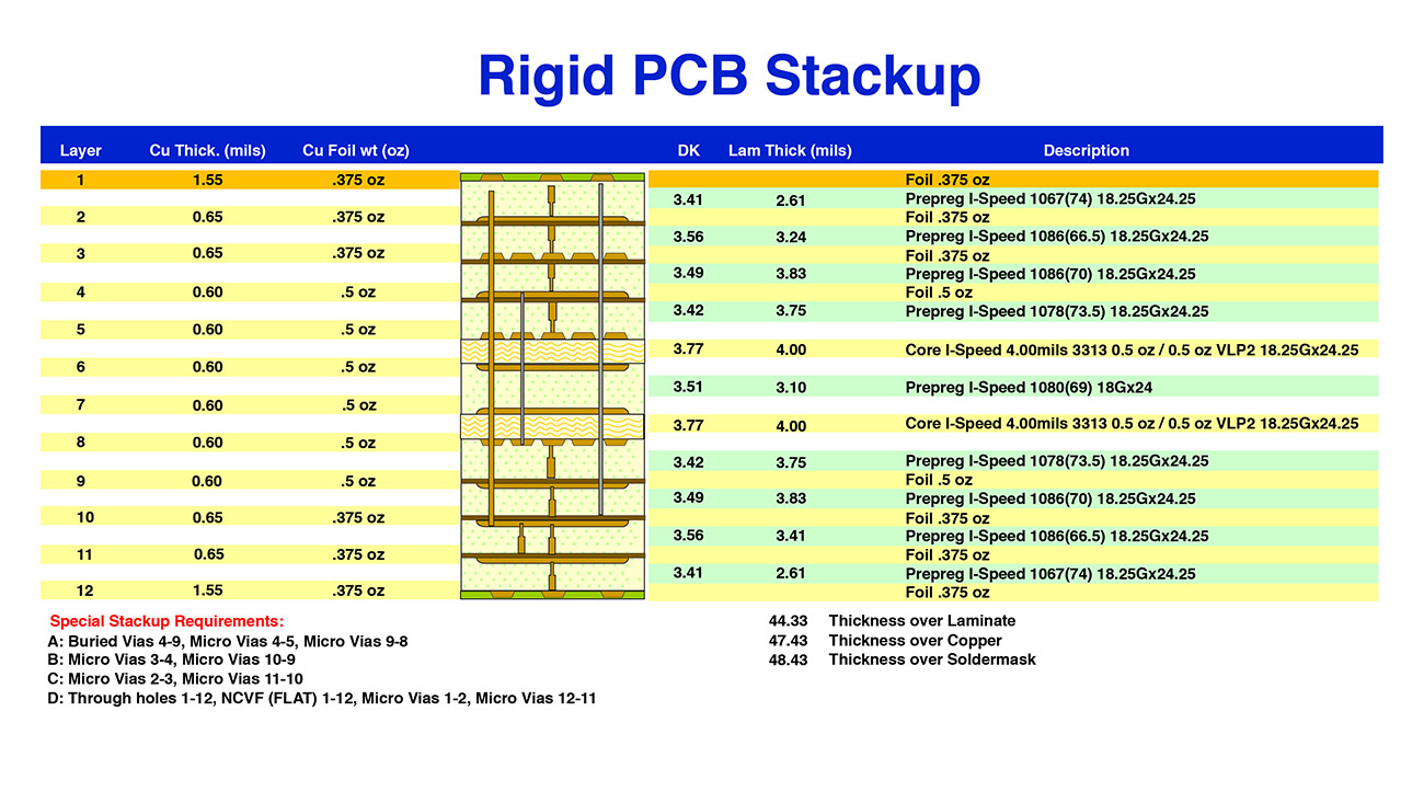
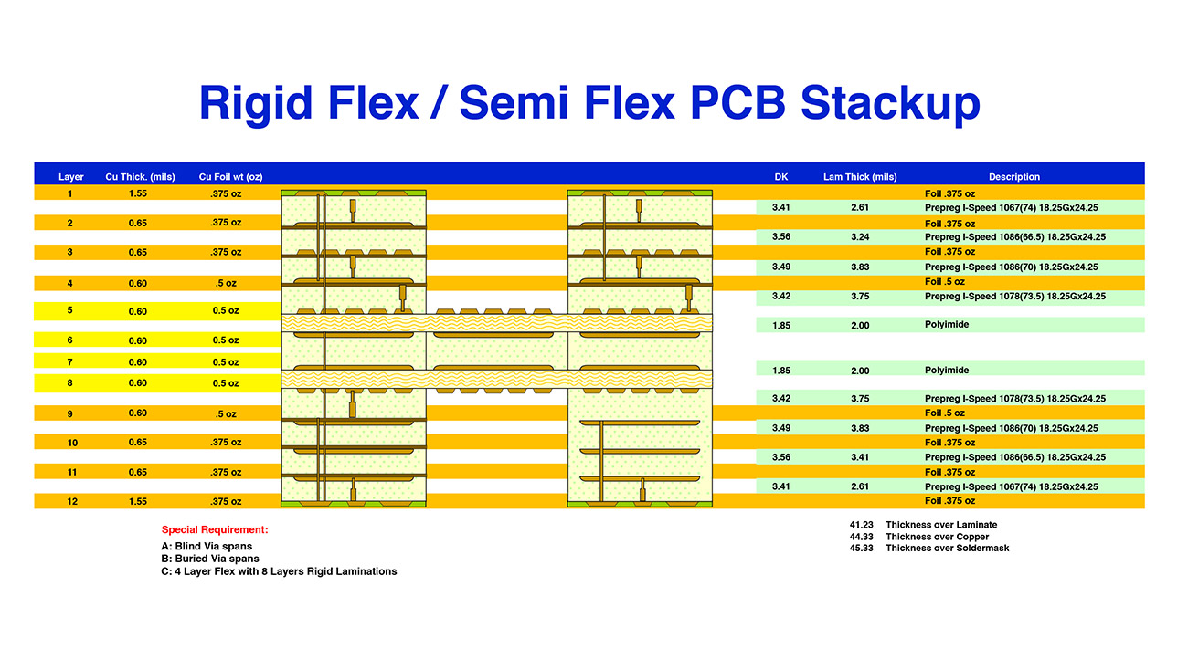
In HDI PCB manufacturing, the stack of layers plays a critical role in ensuring optimal performance. A well-designed HDI board incorporates internal layers and stacked microvias that allow for high-density routing and efficient signal transmission. At Blind Buried Circuits, our engineers carefully plan the HDI board stack up, ensuring that each layer is precisely configured to meet the specific needs of your device, whether it’s for mobile technology or high-speed data transmission.
HDI PCB vs Traditional PCB
UNDERSTANDING HDI BOARD STACKUP FOR ENHANCED PERFORMANCE
In HDI PCB manufacturing, the stack of layers plays a critical role in ensuring optimal performance. A well-designed HDI board incorporates internal layers and stacked microvias that allow for high-density routing and efficient signal transmission. At Blind Buried Circuits, our engineers carefully plan the HDI board stack up, ensuring that each layer is precisely configured to meet the specific needs of your device, whether it’s for mobile technology or high-
speed data transmission.
ADVANCED HDI MANUFACTURING WITH SEQUENTIAL LAMINATIONS
At Blind Buried Circuits, we utilize cutting-edge techniques such as sequential laminations in our HDI manufacturing process. This method allows us to achieve higher circuit densities and improved performance, which is critical for industries requiring compact and powerful electronic designs. By incorporating microholes and other advanced fabrication techniques, we can create high-performance HDI PCBs that meet the demands of modern electronic devices.
HDI PCB Advantages
- Increased component density: For compact electronic devices, the circuits require a large number of components in a limited area. HDI PCBs can accommodate complex designs in limited areas.
- Better signal integrity: For high-speed boards, signal loss and electromagnetic interference play a vital role in the functionality. HDI PCBs provide better reliability and performance for signal integrity circuit designs.
- Improved thermal management: With the help of better routing density, the HDI circuit designs provide optimal head dissipation and better functioning of electronic components.
- Higher interconnection reliability: using the blind buried vias technology in the HDI PCB designs ensures strong multiple-layer connections and reliable manufacturing between conductive layers.
For designs requiring complex interconnections, BGA fanout, and ELIC PCB (Every Layer Interconnect) technologies provide a solution to manage dense component placement while ensuring reliable connections. At Blind Buried Circuits, our HDI manufacturing process can support the most challenging layouts, including vaporize shrink melt techniques to manage heat dissipation. These advanced processes allow us to meet the stringent requirements of
industries like aerospace, automotive, and medical devices.
HDI PCB Applications
Blind Buried Circuits have served several customer needs for their HDI designs and delivered the highest quality possible. All mobile devices, including smartphones, tablets and wearable devices, require HDI PCBs. It is also used in various industries with an increased demand for smaller, thinner and more powerful devices.
- Mobile Devices: HDI PCBs are widely used in the mobile industry, offering a small and convenient size with high-density interconnections.
- Medical Devices: HDI PCBs enable advanced and smart healthcare solutions for various medical devices.
- Aerospace and Defence Systems: HDI PCBs are considered the most reliable PCBs compared to the other PCB types. Most of the aerospace and defence critical devices rely on HDI PCBs.
- Automotive Electronics: With the increase of electric vehicles, and complex designs, HDI accommodates enhanced functionality and optimizes space utilization.
- Industrial Automation Systems: HDI PCBs’ compact size and strong connectivity advantages help control and monitor the systems efficiently.
MEETING INDUSTRY STANDARDS FOR HDI PRINTED CIRCUIT BOARDS
At Blind Buried Circuits, our HDI PCB designs adhere to strict industry standards, ensuring that every HDI printed circuit board we manufacture meets the highest quality and reliability expectations. We comply with IPC and other international standards to deliver PCBs that function reliably in critical environments such as defense systems, medical devices, and
industrial automation. This commitment to quality ensures long-lasting performance and safety in all applications.
EFFICIENT LAYER STACKUP FOR HIGH-DENSITY INTERCONNECT SOLUTIONS
The layer stack up in HDI PCBs determines how well the board can handle high-density connections. Blind Buried Circuits uses sophisticated techniques to optimize the stacking process, ensuring minimal signal loss and maximum efficiency. Our stacked micro vias ensure strong connections between internal layers, making our HDI PCBs ideal for high performance applications in industries such as telecom and industrial automation.
HDI PCB Manufacturing and Production Process
The manufacturing process of HDI PCBs at Blind Buried Circuits includes various stages, which help complete the project with the highest quality standards and customer satisfaction.
The HDI PCB Manufacturing and Production Process include:
- Creating layout design: drawing the schematic and BOM.
- Generating the Gerber file
- Choosing the materials
- Preparing the core and stacking the layers
- Etching the inner-copper layers
- Layer stack up with vias formation
- Drilling process for microvias, buried vias, and blind vias
- Outer layer etching using photoimaging
- Copper deposition and plating
- Applying solder mask and silkscreen
- Electrical Testing
- PCB Assembly
- Quality check and inspection.
- Double AOI and Inspection.
- Packing and delivering
With the robust manufacturing and assembly process, we provide our customers high-density interconnect PCBs within the committed lead time.
Request your HDI Circuit manufacturing Quick Turn Pricing Today!
For your HDI PCB design manufacturing and pcb assembly, contact us today for the HDI PCB price. We’re here to meet your specific requirements.

