Request our manufacturing capability
Capabilities
Printed Circuit Board Substrate Materials - PCB Substrates
Precision Layouts. Proven Performance.
Our Capabilities
Printed Circuit Board Substrate Materials - PCB Substrates
PCB Substrates in USA and Canada:
The PCBs are composed of non-conductive laminates, conductive metal films, and (dielectric material). Blind Buried Circuits stock laminates that are accomplished from substrate materials such as;
- Ceramic
- Composite Epoxy Materials (CEM).
- FR-4
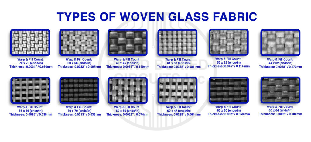
Wide Range of Different Dielectric Materials Circuit Board:
A dielectric material is most frequently made up of fiber weave and epoxy resin (sometimes unwoven). These materials may add an amount of ceramics to enhance the dielectric constant which is also known as PCB Substrate. Blind Buried Circuit offers a wide range of dielectric materials which helps you in selecting the right substrate material considering the chemical properties, mechanical properties, and thermal properties of a PCB (Printed Circuit Board). If your design requires better thermal execution then we always recommend going for a ceramic-based substrate.
Different Properties of PCB Substrate:
PCB board material, also called Dielectric material, delivers electrical insulation among the conductive layers. The properties of these dielectric objects (materials) affect the execution of a PCB under various operating conditions, such as high temperature and high frequency.
At Blind Buried Circuits, we generally classify the different properties of PCB substrate into the following;
- Chemical properties
- Electrical properties
- Mechanical properties
- Thermal properties
1) Effects of Chemical Properties:
The chemical properties of the dielectric material affect the electrical and thermal properties of the board, and it also affects the capacity of the board to resist CAF (Conductive Anode Filament) formation. Some of the chemical properties are described below:
Resistance of Methylene Chloride: The capacity of a material to resist methylene chloride consumption is called methylene chloride resistance. It is expressed by the percentage enhancement in the density of a circuit board material due to soaking or exposure to methylene chloride under controlled situations. Most of the materials have a value of methylene chloride in the range of 0.01% to 0.20%.
Moisture Consumption: The capacity of a substrate to water consumption when absorbed in water is called moisture consumption. It is given by the percentage enhancement in the density of a PCB (Printed Circuit Board) material due to water consumption under controlled situations as per criteria test procedures. Most of the materials have values of moisture consumption in the range of 0.01% and 0.20%.
2) Effects of Electrical Properties:
The electrical properties of a PCB substrate include:
Dissipation Factor or Dielectric Loss Tangent (Df or tan δ): A material’s loss tangent gives a measure of the power absent due to the material. The material loss tangent is directly proportional to the power lost. The lower the material’s loss tangent, the minor will be the power loss.
Relative Permittivity or Dielectric Constant (ER or DK): Contemplate the dielectric constant of a material is essential for signal impedance and signal integrity requirements, which are captious factors for high-frequency electrical performance. The dielectric constant for most PCB (Printed Circuit Board) materials for lower boards is in the range of 3.2 to 3.6; for higher frequency boards, the dielectric constant is in the range of 2.5 to 4.5.
3) Mechanical Properties:
The mechanical characteristics of a material determine its capacity to combat exterior loads without losing its properties. Some of the mechanical properties are discussed below:
Elastic Modulus or Tensile (Young’s) Modulus: It is a measure of the hardness of a solid material or the quantity of force necessary to disfigure a material. It is described as the ratio of the stress (force per unit area) under an axis to the strain (ratio of deformity over basic length) along that axis in the range in which Hooke’s Law grips good, i.e., the stress-strain curve is linear. It is expressed as pounds/square inches (Psi) or pascals.
Tensile Strength: It is an estimate of a material’s greatest stress it can take before breaking while being pulled from both sides. It is expressed as pounds/square inches (Psi) or pascals.
Peel Strength: A measure of the bond strength between the dielectric material and the copper conductor is called Peel Strength. It is expressed in (PLI) pounds of force per linear inch.
Bend Strength or Flexural Strength: A measure of a material’s capability to combat mechanical stress without fracturing when a PCB (Printed Circuit Board) is backed at the ends and in the center it is loaded.
4) Thermal Properties:
The thermal properties of a PCB (Printed Circuit Board) substrate play an essential role in the stage of assembly. These thermal properties are as follows:
Decomposition Temperature (TD): The temperature at which a material chemically decays (the material loses about 5% of mass). It is known as TD (decomposition temperature).
Glass Transition Temperature (TG): The temperature range in which a substrate changes from a rigid, glassy state to a deformed, softened state as polymer chains become more mobile. It is called TG (glass transition temperature).
A material’s TD is an essential factor when assembling PCBs (Printed Circuit Boards) because when a material surpasses or reaches its TD, changes to its characteristics are not reversible. This is in contrast to TG, where characteristics will reverse to their original states once the materials cool down the TG range.
We help you select the right material that can work in a temperature range that is greater than the TG but well less decomposition temperature (TD). Our experienced process engineers ensure that the board material is compatible with the solder temperature during the assembly process. We recommend the material TD to be greater than 200°C to 260°C.
Types of PCB Materials:
All the board laminates are of different types which include CEM1 through CEM5, FR-1 through FR-6, G-10, and G-11 materials. We generally stock pcb circuit board materials such as FR-4, Megatron 6, Isola 370HR, FR408HR, Rogers, tachyon 100g, and other low coefficient DK & DF pcb adhesive material as a substrate material for rigid PCB (Printed Circuit Board) fabrication and are capable of arrange other special materials as per your requirements.
Why FR-4 is applied as a Substrate?
The FR-4 is an alternative to fire retardant material that is applied in board fabrication. In the present electronic manufacturing industry, FR-4 substrates are widely used. Blind Buried Circuits Inc fabricates multilayered, double-sided, and single-sided boards with FR-4 material. Some of the qualities of FR-4 materials that made the FR-4 popular are mentioned below:
- Higher TG value (about 180°C).
- Offer decent mechanical properties to control board structure integrity.
- Offer operating temperature from (50°C to 115°C).
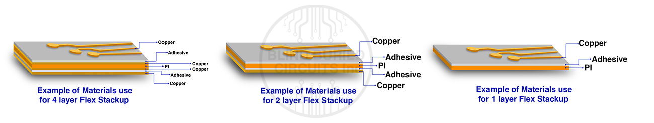
Substrate for Flex PCB (FPCB):
The flexible PCB boards demand a substrate material that can be twisted and folded without breaking. Blind Buried Circuits use polyimide material and various adhesive for PCB as a substrate in flex PCBs. The compactness of these materials does not extend 120µm and plays an essential role in the design of the board. Our engineers always consider mechanical and temperature requirements while choosing a substrate material.
Exotic Material Capabilities:
Send us an RFQ (Request for Quote) now at our website and get a custom quotation for reliable exotic material PCBs. At Blind Buried Circuits, we manufacture exotic HDI PCBs and deliver it to all over the USA and Canada.


Ready To Get Started?
Reach out to us at sales@blindburiedcircuits.com or call as at USA: +1 (281) 654-8963 to get further information about PCB Substrate! Feel free to fill our inquiry form to get a quick quotation.

