Request our manufacturing capability
Capabilities
PCB Layout Design
Precision Layouts. Proven Performance.
Our Capabilities
PCB Layout Design
Get Your High-Speed PCB Design Started Today with Blind Buried Circuits
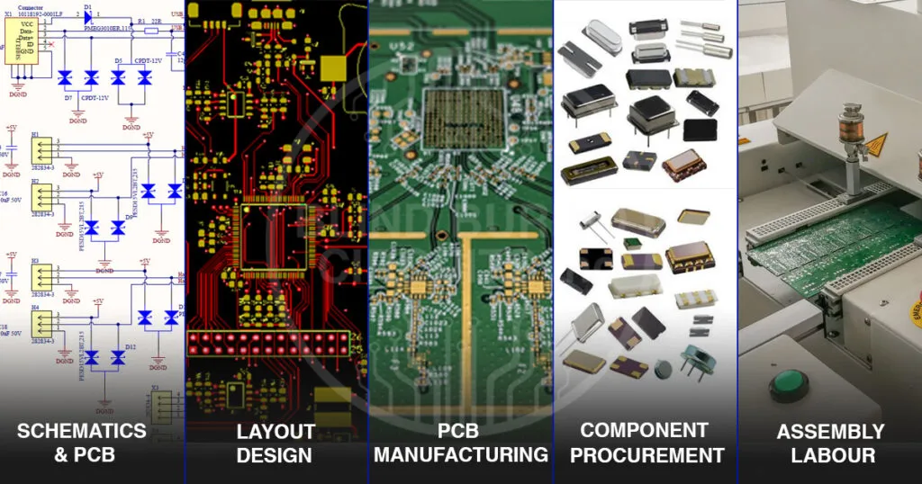
Blind Buried Circuits offer Full Turnkey services for PCBs from 2 to 60+ layers and anything in between. Our services include:
- PCB Designing
- Design Verification
- PCB Manufacturing
- Component Procurement
- PCB Assembly
As a one-window service provider with a decade of experience and experienced electrical engineers specializing in PCB design for IoT, Medical Devices, Automobile, Telecommunication, and Consumer electronics, we offer guidance on design optimization and material selection to help reduce the risk of errors and design flaws as an add-on service.
Introduction to PCB Design
PCB Design Process Flow
PCB design process flow involves:
- Gathering the circuit requirements
- Schematic Design
- Selection of Components (Surface mount technology (SMT) and Through-hole technology (THT))
- PCB Stackup Design
- PCB Layout Design and Placement of Components
- Verification of PCB Design Techniques based on the PCB Design Guidelines (PCB Design for Manufacturing (DFM) and Design for Assembly (DFT / DFA))
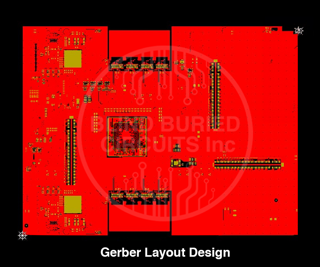
- Final Manufacturing files generation (Gerber files, solder mask files, silkscreen files, Bill of Material (BOM), PCB fabrication Drawings, PCB Assembly Drawings, Vias and Drill Data, Design Database)
Once all the above requirements are fulfilled, our team will provide PCB manufacturing and PCB assembly quotation and procure parts from our approved vendor list.
EDA / CAD / CAM Tools and Software for PCB Design
- Altium Designer
- Mentor Graphics – PADS
- Cam 350
- Eagle
- Genesis 2000
PCB Design Checklist
Step 1: Define the Circuit Requirements
- Schematic Diagram (Softcopy in PDF or hand drawn)
- Bill of Material (BOM) with complete manufacturing part numbers in XLS or Excel format.
Step 2: Define the Printed Circuit Board's mechanical dimensions
- PCB shape and size
- Critical component placements (if any)
- Mechanical constraints of the final product (if any)
Step 3: Define the critical design constraints
- To take care of EMI/EMC shielding and thermal Interface, you need to provide what environment the PCB will place.
- Does the design require Impedance control, high-speed PCB design copper traces, or special requirements?
- Is there any no-go or keep-out area?
- For determining PCB parameters like copper thickness, and cutouts, we will need to know the maximum voltage/current requirements in PCB.
- Any other special instructions which need to follow?
Step 4: Determine the expected layer count
Step 5: Final review of requirements and quotation process
Step 6: Placing your Order
Finally, you’re ready to place the order for PCB Layout Design. Please submit your request to sales@blindburiedcircuits.com, and our accounting team will contact you for payment details.
As soon as the payment gets cleared, our team will start the PCB Layout Designing, and once the design gets completed. We will send you the Gerber files (including the solder mask and silkscreen files) and others documents.


Ready To Get Started?
To learn more about our PCB Design Guidelines, don’t hesitate to contact our sales team at sales@blindburiedcircuits.com.

