Request our manufacturing capability
Industries We Serve
Printed Circuit Boards For Telecom PCB
TELECOMMUNICATION PCB

PRINTED CIRCUIT BOARD USAGE IN TELECOMMUNICATION PROJECTS:
- Manufacturing of GPS devices PCB (Printed circuit board) assembly.
- Prototype and mass production of USB Controllers.
- Prototype and production quantity assembly of cell phones PCB (Printed circuit board) prototype to production.
- Prototyping of modem PCBs (Printed circuit board).
- Prototype Broadband PCB and PCBAs (Printed circuit board assembly).
- Prototype EPABX System PCB (Printed circuit board).
- PCB layout of Ethernet Cards.
- Prototyping of Customized Telecommunication PCB (Printed circuit board).
- Satellite PCB Assembly.
- Telephone Exchange PCB Assembly.
- Ethernet / Giga Byte Switches PCB Assembly.
- Prototyping of VOIP Adapter PCB (Printed circuit board).
- Wired Internet / Fiber Router PCB Prototype.
- VOIP Modem PCB (Printed circuit board) Assembly.
- 11 a/b/g/n cellular Router PCB (Printed circuit board) complete assembly.
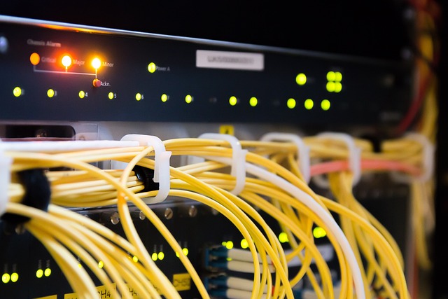
TESTING STANDARDS FOR TELECOMMUNICATION PCB:
Blind Buried Circuits has been certified and follows ISO 9001:2015 quality management systems (QMS) that assure zero-defect manufacturing. We pursue the stringent manufacturing criteria as per IPC class 2 and 3 guidelines. This means constant analysis at each step of the manufacturing process, such as;
- Solderability testing: Assures that the solder has properly attached to the surface of the circuit boards.
- Automated Optical Inspection (AOI): AOI ensnares images of the PCB (Printed Circuit Board) with either a single 2D camera or two 3D cameras. The ensnared image is correlated with the schematic. If the boards are not identical to the schematic, then the boards are transferred to manual scrutinize.
- Ionic Contamination Testing: The ionic contamination testing is accomplished to detect ionic debris resulting from the production and soldering procedures.
- Flying Probe Test for Fabrication and Assembly: The test probes cover the distance from one point to another, quickly examining for shorts, opens, and other issues with the PCBs (Printed Circuit Boards).
- Peel Strength Test: It settles the measure of strength needed to peel the laminate from PCB (Printed Circuit Board).
- First Article Inspection (FAI): The verification of around one to three pieces after the fabrication starts in a manufacturing dexterity is called as FAI (First Article Inspection). FAI is commonly performed for devices that call for a high-level correction.
- Time-Domain Reflectometry (TDR): TDR measurements are essential for assuring signal integrity. Signal integrity is authenticated by testing for electrical cessation in the communication line channel and connectors.
- X-Ray Fluorescence (XRF): This test is applied to determine the surface finish covering compactness of the board (such as for ENIPIG or ENIG covering).
- Micro-Sectioning Tests: A Micro-sectioning analysis is a form of destructive testing that is carried out to settle the PCBs (Printed Circuit Boards) and spot internal defects. The defects detected can range from barrel cracks, pad-lift corner cracks, Z- axis expansion, and more. It can also settle the copper compactness at different regions of the board.
HIGH-AUTHENTICITY DEMAND WITH FULL DETECT-ABILITY:

IPC-A-610H – SOLDERING REQUIREMENTS FOR TELECOMmunication PCB (PRINTED CIRCUIT BOARDS):
Blind Buried Circuits follows electronic assembly criteria, revision H. This accommodates the ESD considerations into a particular addition and arrangement for PCBA (Printed Circuit Board Assembly), contrary to wire and cable equipment. Our aim is to provide our customers in the USA and Canada with ideal operating conditions.
UL 94V-0:
The UL stands for (Underwriters Laboratories). The standard UL 94V-0 deals with plastic flammability and assigns to the standard protection of the flammability of plastic objects for parts in products and appliance testing.
Blind Buried Circuits has manufacturing partners who are UL 94V-0 certified for flex, rigid, rigid-flex, microelectronics, and HDI boards, which assures a high level of flame-blocking properties which puts your boards in good hands.
REPORTS AND CERTIFICATES:
Following certifications and detailed reports for PCBs (Printed Circuit Boards) are provided by Blind Buried Circuits;
- Certificate of conformance for fabrication and assembly
- First article inspection (FAI) certificate.
- Final micro-section Report.
- Open and short electrical test report.
- Hole and dimension measurement report.
- Impedance measurement TDR report.
- Reliability test report.
FULLY ASSEMBLED PCBS (PRINTED CIRCUIT BOARDS) MANUFACTURED IN THE USA AND CANADA FOR ALL YOUR TELECOM REQUIREMENTS:
- DFA and DFM Analysis on every Board: Live engineering abutment and software accelerated tests on all orders.
- Extensive Electrical Analysis: AOI, Flying Probe, BGA, X-ray, and Cross-Section to name a few.
- FAB + Assembly Under One Roof: Avoid loiters by applying a single vendor for PCB assembly, component procurement, design analyses, and PCB fabrication.
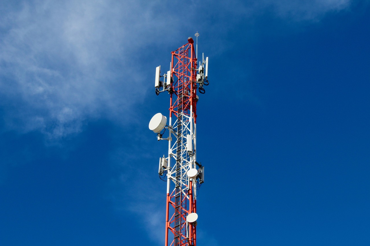
APPLICATIONS OF TELECOMmunication PCB:
- Mobile devices.
- Network management system.
- Wireless Networking.
- Telecom infrastructure.
- Maintenance and Customization.
- IT support.
- IT application development.
- Space communications technology.
- Satellite Technology.
- Wireless industrial and commercial phone technology.
- Signal boost online systems.
- Video collaboration.
- PBX systems.
- Phone switching systems.
- Cell transmissions and tower electronics.
- Voice over internet protocol.
- High-speed routers and servers.
- Information security technology.
HOW TO GET A QUOTE FOR TELECOMmunication PCB:
If you want to get a quick quotation for the PCB, please reach us at sales@blindburiedcircits.com or to get more information about telecommunication PCB and prototypes, call us at USA: +1 (281) 654-8963. In order to give you a quick quote, we require the following information:
- BOM
- Gerber or ODB++
- Required Turn time.
- Required Quantity.
All the highest quality IPC Class 2 and 3 PCBs are delivered in Canada and USA.

