Request our manufacturing capability
Capabilities
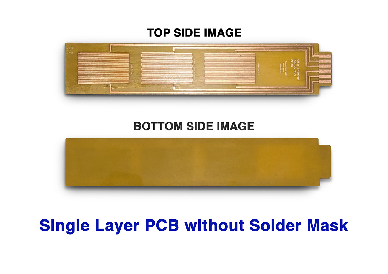
Single Layer PCB
Precision Layouts. Proven Performance.
Our Capabilities
Single Layer PCB
What Is Single Layer PCB?
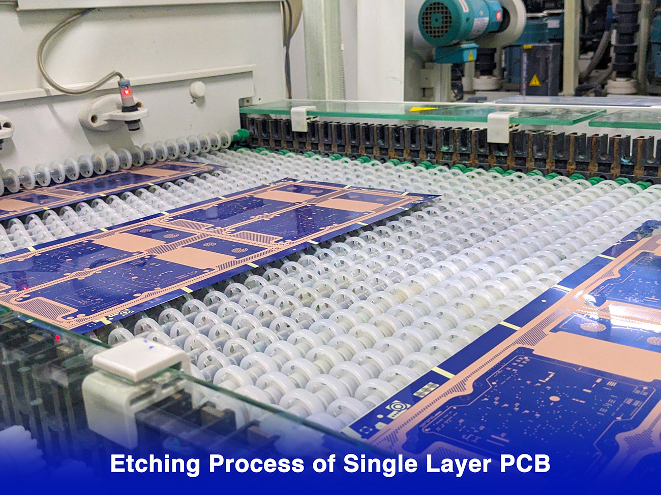
A single layer PCB is type of PCB that is made of substrate material which is typically fiber glass or an equivalent material with conductive copper channels. Traces are used to link the various components that are installed on the board of single layer PCB. Single layer PCBs are usually made for simplest electrical devices for simple circuitry. Single layer PCBs hold a unique position due to their less expensive in cost then multilayer PCB’s. Below are the mentioned capabilities, detail structure and application about single layer PCB’s
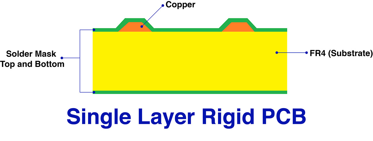
The Single Layer PCB Structure
The single layer PCB is consist of only one sided copper (conductive copper) over the non conductive PCB substrates. Below is the overview of its structure:
Substrate (Base Material)
Substrate is a base material made from epoxy resin fiber glass, which helps as a mechanical support for rigid PCB’s, current insulation and helps keep all copper layer separate.
Copper Layer
Solder Mask
A polymer layer that is usually green, also it comes in other colors. It protects the copper traces from oxidation and prevents solder bridges between solder pads during the soldering process.
Silkscreen
A non-conductive ink, often white, but can also be yellow, black, or other colors. The purpose for printing silkscreen on PCB’s is to provide reference designators, UL & Date code markings and other information to help during assembly and troubleshooting.
Stackup of Single Layer PCB's
- Signal Integrity
- EMI/EMC Considerations
- Power Distribution
- Component Placement and Routing
- Thermal Management
- Reliability and Long-term Performance
- Mechanical Strength and Durability
- Manufacturability and Cost Constraints
Applications & industries of Single Layer PCBs
- Consumer Electronics
- Automotive Electronics
- Home Appliances
- Educational and Prototyping Purposes
- Communication Devices
- Audio Devices
- Toys and Gadgets
- Lighting Solutions
- Office Equipment
Single-layer PCBs are still essential in many applications where easy application, cost, and fast response are important considerations. Engineers and producers must comprehend their applications, structure, and stack-up details. By using their strengths through thoughtful design and consideration, one can successfully utilize the advantages of single-layer PCBs in different applications including, home appliances, educational and prototyping purposes.


Ready To Get Started?
We welcome you to send a custom design/manufacturing quote for your current project to our experienced sales engineers at sales@blindburiedcircuits.com and aly@blindburiedcircuits.com. We are committed to fulfill your critical or standard design & manufacturing requirement with our IPC Certified Workmanship. And to ensure your electronic initiatives comes to a success.

