

Request our manufacturing capability
Capabilities
High Volume PCB Assembly
Our Capabilities
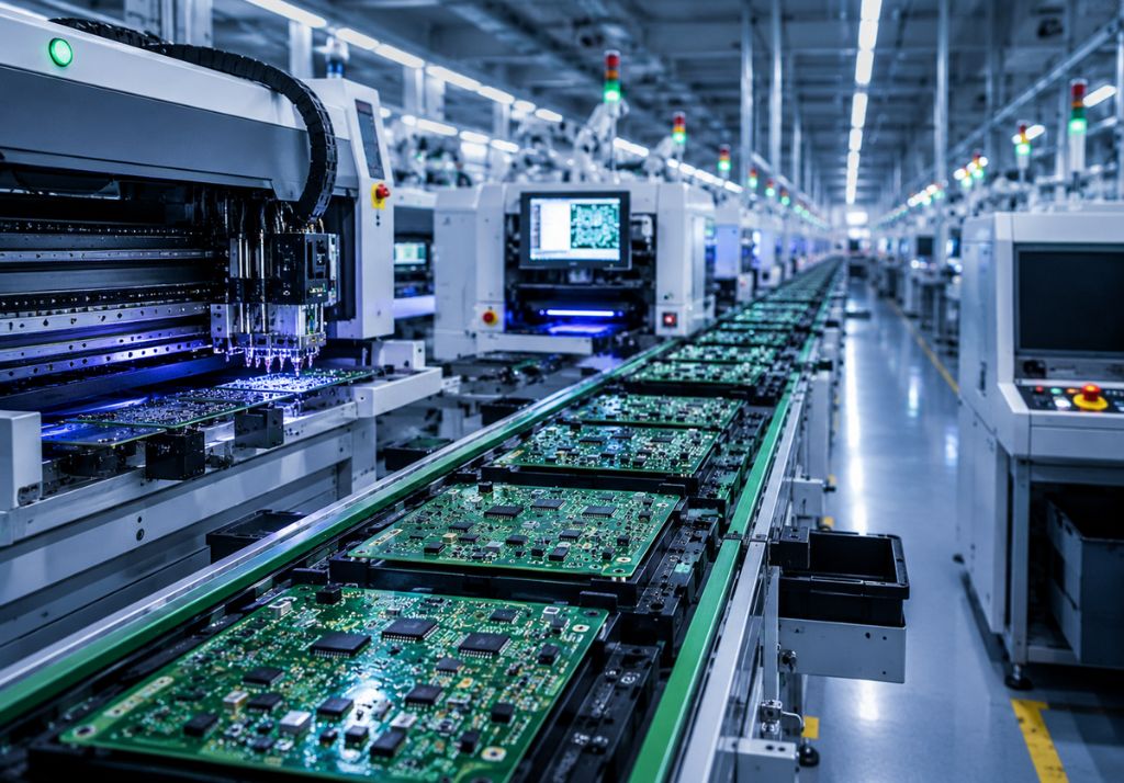
As electronic products move from validation to full-scale production, manufacturing consistency becomes critical. A design that performs well in a prototype environment must maintain the same performance across thousands or even millions of assemblies. At Blind Buried Circuits, we provide high volume PCB assembly services for OEMs that require repeatable quality, predictable yields, and cost-effective production at scale. Our manufacturing processes support RF, digital, mixed-signal, power electronics, and high-density interconnect designs through automated production systems and controlled manufacturing workflows. Our high-volume electronic PCB assembly capabilities combine advanced SMT equipment, statistical process control (SPC), traceable manufacturing records, and comprehensive inspection procedures. Whether you require tens of thousands of units or sustained multi-million-unit production, we help ensure consistent assembly quality throughout every stage of high-volume PCB production.
High Volume PCB Assembly Services Offered by Blind Buried Circuits
As an experienced provider of high-volume PCB manufacturing services, Blind Buried Circuits offers comprehensive assembly solutions that support large-scale production requirements while maintaining strict quality standards.
- Automated SMT Assembly: Our surface mount technology production lines are optimized for high-speed automated assembly for high volume PCBs. Advanced pick-and-place systems support fine-pitch components, BGAs, micro-BGAs, QFNs, CSPs, and other complex package types with consistent placement accuracy and throughput.
- Through-Hole and Mixed Technology Assembly: Many industrial and power electronic products require a combination of surface mount and through-hole components. We support mixed-technology assemblies using selective soldering, wave soldering, and automated inspection processes to ensure reliable results across large production volumes.
- HDI and Blind/Buried Via PCB Assembly: As specialists in advanced circuit board manufacturing, we assemble HDI designs featuring blind vias, buried vias, stacked microvias, and fine-pitch component packages. These assemblies are commonly used in telecommunications, aerospace, medical, and high-performance computing applications.
- Turnkey High Volume PCB Assembly: Our turnkey manufacturing services simplify the production process by managing PCB fabrication, component sourcing, assembly, inspection, testing, and logistics through a single manufacturing partner. This approach improves supply chain coordination and reduces procurement complexity.
- High Volume Quick Turn PCB Assembly: When production schedules are compressed, OEMs need a manufacturing partner that can respond efficiently. Our high-volume quick turn PCB assembly services support accelerated production requirements while maintaining process control, quality standards, and delivery performance.
- Design for Manufacturing (DFM) Support: Before production begins, our engineering team reviews design files to identify opportunities for manufacturing optimization. DFM analysis helps improve assembly efficiency, reduce defects, and increase production yields before the first board enters the assembly line.
- Component Procurement and Supply Chain Management: Large-scale manufacturing depends on stable component availability. We work with approved suppliers and authorized distributors to secure components, monitor lifecycle risks, and support uninterrupted high volume PCB production.
High Volume PCB Assembly Process
Successful high volume PCB assembly requires a controlled manufacturing process that minimizes variation and supports repeatable production outcomes. Our workflow is structured to improve efficiency, maintain quality, and support long-term production programs. Here are the key stages of our high-volume PCB assembly process:
- Design Review and Production Planning: The process begins with a detailed review of Gerber files, ODB++ data, assembly drawings, BOMs, and testing requirements. Our engineers evaluate the design for manufacturability, assembly compatibility, and process stability.
- Material Procurement and Inventory Management: Component availability, supplier qualifications, lifecycle status, and lead times are reviewed before production begins. Strategic inventory planning helps support uninterrupted high volume PCB manufacturing schedules.
- PCB Fabrication Verification: Incoming circuit boards undergo verification to confirm compliance with approved specifications. Critical features such as controlled impedance structures, blind vias, buried vias, layer registration, and surface finishes are evaluated before assembly.
- Solder Paste Printing and SPI: Automated stencil printing systems apply solder paste with controlled deposition volumes. Solder Paste Inspection (SPI) verifies paste quality and placement accuracy before component mounting.
- High-Speed Component Placement: Advanced pick-and-place systems perform high-speed automated assembly while maintaining precise component positioning. Production programs are optimized to maximize throughput and repeatability.
- Reflow and Soldering Operations: Controlled thermal profiles ensure proper solder joint formation and component integrity. Depending on assembly requirements, boards may undergo reflow soldering, selective soldering, or wave soldering processes.
- Automated Inspection and Testing: Quality verification occurs throughout production using multiple inspection technologies, including:
- Solder Paste Inspection (SPI)
- Automated Optical Inspection (AOI)
- X-ray Inspection
- In-Circuit Testing (ICT)
- Functional Circuit Testing (FCT)
These inspection methods help identify process variations before they affect production yields.
- Final Validation and Traceability: Completed assemblies undergo final quality verification before shipment. Manufacturing records, inspection data, lot tracking information, and testing documentation are maintained to support full traceability throughout the product lifecycle.
Key Advantages of Our High-Volume PCB Assembly Services
Large-scale manufacturing offers significant operational and cost advantages when supported by controlled production processes and proven assembly expertise. Following are the key advantages of our high-volume PCB assembly services:
- Consistent Product Quality: One of the primary benefits of high-volume PCB assembly is manufacturing repeatability. Automated production equipment and SPC monitoring help maintain consistency across every production lot.
- Lower Cost Per Unit: As production quantities increase, manufacturing efficiencies improve. Optimized panelization, automated assembly workflows, and streamlined production scheduling contribute to lower assembly costs.
- Improved Production Yield: Process controls, inspection technologies, and manufacturing data analysis help reduce defects and improve overall production performance.
- Scalability for Growing Production Demands: Our high-volume PCB assembly services make it easy to increase production as demand grows, helping manufacturers meet larger order volumes while maintaining consistent quality and delivery schedules.
- Enhanced Traceability and Quality Control: Comprehensive production records, lot traceability, and quality documentation improve process visibility, support compliance requirements, and provide greater confidence in every production run.
Applications and Industries We Serve
Blind Buried Circuits supports high volume electronic PCB assembly across industries where reliability, performance, and manufacturing consistency are critical.
- Aerospace & Defense: We manufacture assemblies for avionics, communication equipment, navigation systems, and mission-critical electronics that require IPC Class III workmanship standards.
- Automotive & Electric Vehicles: Our high-volume PCB assembly services support battery management systems, vehicle control modules, sensors, power electronics, charging systems, and EV infrastructure technologies.
- Telecommunications & 5G: We assemble high volume PCBs for telecommunications equipment, networking hardware, RF modules, and 5G infrastructure, ensuring reliable assembly for designs with controlled impedance and high-speed signal requirements.
- Medical Devices: Medical electronics demand traceability, reliability, and process consistency. Our assembly support diagnostic systems, patient monitoring devices, wearable technologies, and other healthcare products.
- Industrial Automation: We assemble high volume PCBs for industrial control systems, robotics, instrumentation equipment, and factory automation platforms that require consistent quality and reliable production at scale.
- Consumer Electronics & IoT: Our high-volume PCB assembly services support consumer electronics and IoT devices with compact layouts, and high component density.
- Renewable Energy: We manufacture assemblies for solar equipment, battery storage systems, power conversion products, and energy management technologies.
- Semiconductor Equipment & Test Systems: Our high-volume PCB assembly services support semiconductor equipment, evaluation boards, and test systems that require fine-pitch BGAs, dense PCB layouts, and precise assembly processes.
- Research & Innovation/New Product Introduction (NPI): OEMs preparing for commercial product launches rely on our manufacturing expertise to support smooth transitions from pilot production to sustained high volume PCB production.
Quality Assurance & Compliance
- PCB shape and size
- Critical component placements (if any)
- Mechanical constraints of the final product (if any)
Step 3: Define the critical design constraints
Quality assurance is integrated throughout every stage of our high-volume PCB assembly process. Rather than relying solely on final inspection, we apply process controls and verification procedures throughout production to maintain consistency and improve yields.
Our quality systems support compliance with recognized industry standards, including:
- IPC-A-610 assembly workmanship requirements
- IPC Class II standards
- IPC Class III standards for high-reliability applications
- RoHS-compliant manufacturing processes
- Statistical Process Control (SPC)
- AOI, SPI, X-ray, ICT, and functional testing methodologies
For blind and buried via assemblies, additional verification procedures evaluate via integrity, board flatness, solder joint quality, and thermal performance before and during assembly operations.
Frequently Asked Questions
High volume PCB assembly typically refers to production quantities large enough to benefit from automated manufacturing optimization, dedicated production scheduling, and economies of scale. Quantities may range from several thousand units to millions of assemblies annually.
Yes. We support ongoing production programs through supply chain planning, inventory management, component lifecycle monitoring, and documented manufacturing processes.
Yes. Manufacturing records, component lot information, inspection results, and testing data can be maintained to support full product traceability requirements.
Yes. We support fine-pitch BGA assembly down to 0.3 mm pitch, along with HDI designs incorporating blind vias, buried vias, and microvia technologies.
We use automated assembly equipment, SPC monitoring, AOI, X-ray inspection, ICT, and functional testing to identify process variations early and maintain consistent production quality.





Ready To Get Started?
To learn more about our PCB Design Guidelines, don’t hesitate to contact our sales team at sales@blindburiedcircuits.com.