

Objective
This blog explains what a PCB stencil is, how it works, the different types available, how PCB stencils are manufactured, and where they are used in electronics manufacturing. You’ll also learn how the right stencil improves solder paste printing, reduces assembly defects, and supports reliable SMT production.
Key Takeaways
- A PCB stencil is used to apply solder paste accurately during SMT assembly.
- The right stencil improves solder joint quality and production consistency.
- Framed, frameless, laser-cut, and electroformed stencils each serve different assembly requirements.
- Proper stencil design, thickness, and alignment help prevent common soldering defects.
- PCB stencils are widely used in prototype, low-volume, and high-volume PCB assembly.
Table Of Contents
- What Is a PCB Stencil?
- Why Is a PCB Stencil Important in SMT Assembly?
- How Does a PCB Stencil Work?
- Why PCB Stencil Printing Accuracy Matters
- Materials Used in PCB Stencils
- Types of PCB Stencils
- How PCB Stencils Are Manufactured
- Applications of PCB Stencils
- How to Choose the Right PCB Stencil
- Common PCB Stencil Printing Problems and Solutions
- Why Choose Blind Buried Circuits for PCB Stencil Services?
- FAQs
What Is a PCB Stencil?
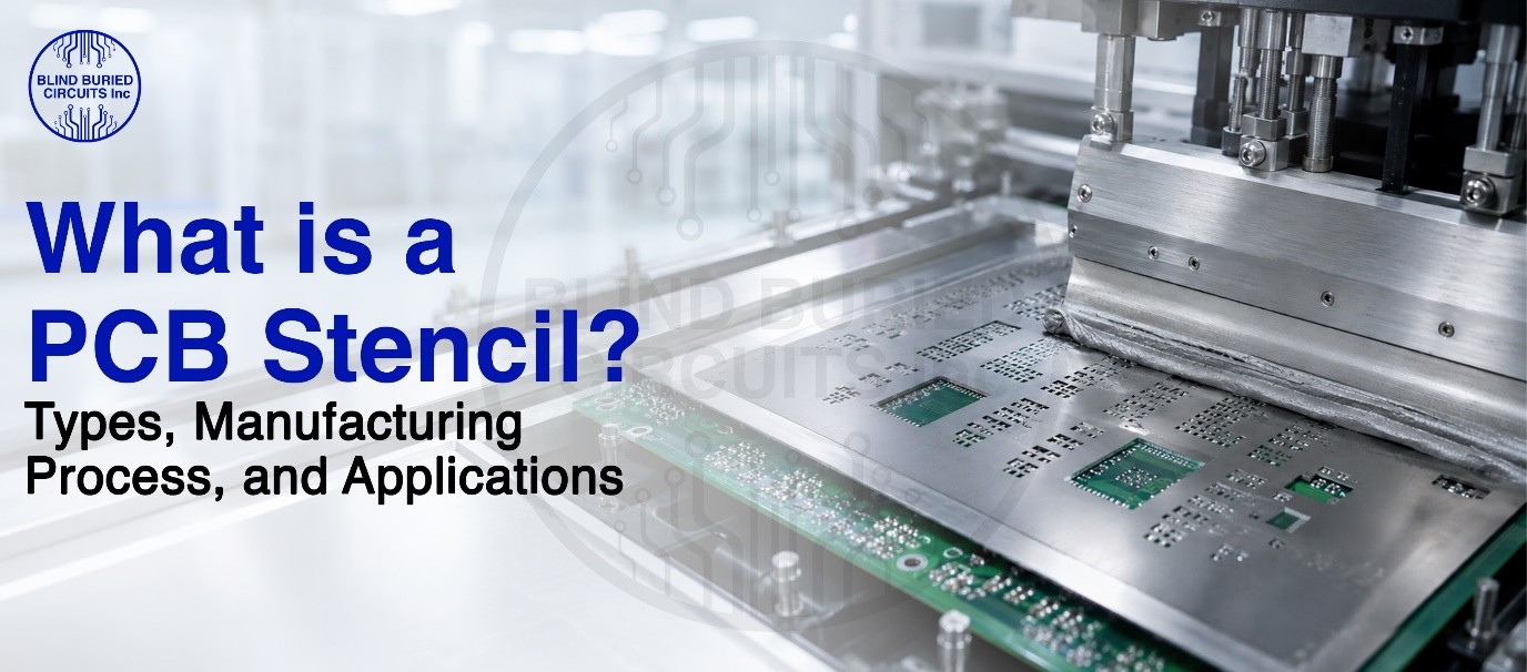
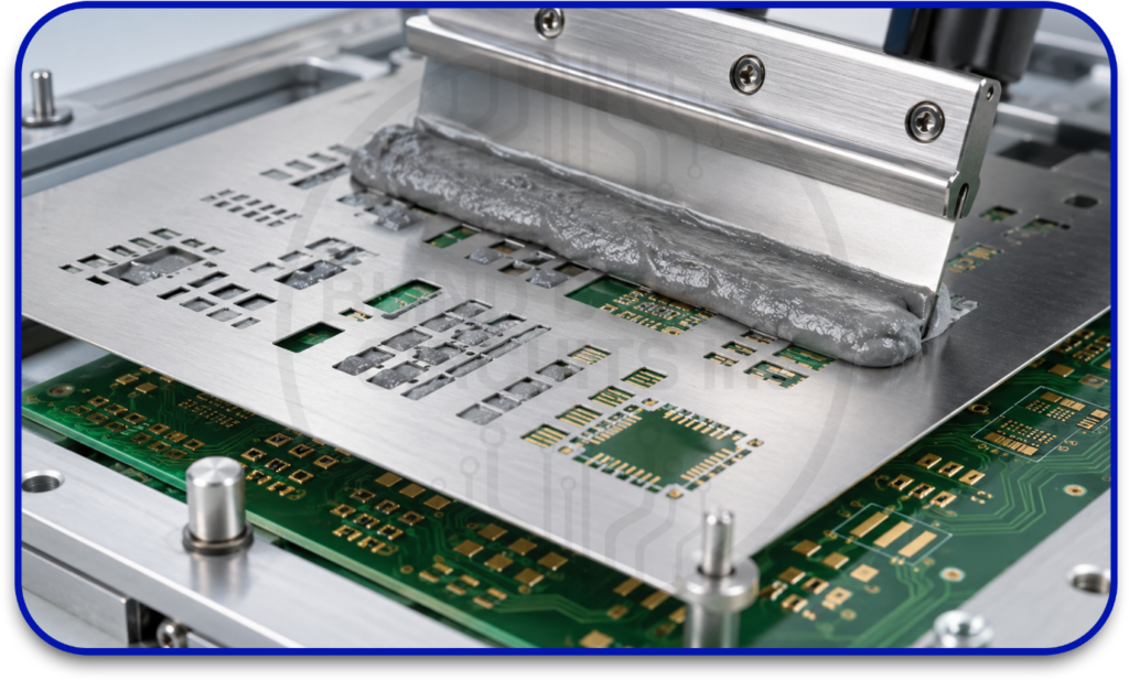
A PCB stencil is a thin metal sheet with precisely cut openings that match the solder pads on a printed circuit board (PCB). During surface mount technology assembly, it is placed over the PCB to apply a controlled amount of solder paste before electronic components are mounted.
Most circuit board stencils are manufactured from stainless steel because it offers excellent durability, dimensional stability, and printing accuracy.
A properly designed stencil for PCB assembly helps you:
- Apply solder paste consistently across every pad
- Improve solder joint reliability
- Reduce assembly defects
- Increase printing accuracy
- Support both prototype and production builds
Without an accurate solder paste stencil, too much paste can cause solder bridging, while too little paste may lead to weak or incomplete solder joints. That’s why stencil quality directly affects SMT assembly performance.
Why Is a PCB Stencil Important in SMT Assembly?
Applying the correct amount of SMT solder paste is one of the most important steps in PCB assembly. Even a small variation in paste volume can affect solder joint quality and component placement.
A high-quality SMT stencil helps ensure every PCB receives consistent solder paste deposits, improving both manufacturing efficiency and product reliability.
Benefits of using a PCB stencil include:
- Accurate solder paste deposition
- Consistent printing across multiple boards
- Faster SMT production
- Reduced soldering defects
- Higher first-pass assembly yield
- Lower rework and material waste
As PCB designs become smaller and more complex, accurate PCB stencil printing becomes even more important. Fine-pitch components such as BGAs, QFNs, and CSPs require precise paste deposition to achieve reliable solder joints.
How Does a PCB Stencil Work?
A stencil in PCB assembly acts as a template that transfers solder paste onto the PCB pads before components are placed.
- Stencil Alignment: The stencil is aligned with the PCB using fiducial marks to ensure every aperture matches the corresponding pad.
- Solder Paste Application: A squeegee spreads SMT solder paste across the stencil surface, filling the laser-cut apertures.
- Paste Transfer: The solder paste passes through the stencil openings and is deposited onto the PCB pads.
- Stencil Removal: The stencil is carefully lifted, leaving uniform solder paste deposits on the board.
- Component Placement: Automated pick-and-place machines position SMT components onto the solder paste.
- Reflow Soldering: The PCB passes through a reflow oven, where the solder pastes melts and forms reliable electrical and mechanical connections.
Why PCB Stencil Printing Accuracy Matters
The amount of solder paste deposited on each pad directly affects assembly quality.
If too much paste is applied, it can cause:
- Solder bridging
- Short circuits
- Component shifting during reflow
If too little paste is deposited, it may result in:
- Weak solder joints
- Open connections
- Poor electrical reliability
A well-designed PCB stencil ensures consistent paste volume across every board, helping manufacturers achieve repeatable, high-quality SMT assembly services.
Materials Used in PCB Stencils
A PCB stencil is designed to withstand repeated printing cycles while maintaining precise solder paste deposition. Most stencils are manufactured from stainless steel, but other materials may be used for specialized applications.
| Material | Features | Typical Applications |
| Stainless Steel | Durable, corrosion-resistant, excellent paste release | Most SMT assembly applications |
| Nickel | Smooth aperture walls, high precision | Fine-pitch and high-density PCB assembly |
| Polyester (Mylar) | Low cost, flexible | Prototype and manual solder paste application |
Types of PCB Stencils
Different PCB stencils are designed for different assembly requirements. The right choice depends on production volume, component density, and printing accuracy.
- Framed PCB Stencil
A framed SMT stencil is permanently mounted to an aluminum frame.
It is commonly used in automated SMT production lines because it provides excellent stability and repeatable printing.
Best suited for:
- High-volume production
- Automated SMT assembly
- Large production runs
- Frameless PCB Stencil
A frameless stencil, sometimes called a foil stencil, is used with a reusable stencil frame.
It offers the same printing accuracy while reducing storage space and overall cost.
Best suited for:
- Prototype builds
- Engineering validation
- Low- to medium-volume production
- Laser-Cut PCB Stencil
Laser cutting is the most common manufacturing method for solder stencils.
A high-precision laser creates clean aperture openings that deliver consistent solder paste deposits across the PCB.
Advantages include:
- Excellent dimensional accuracy
- Smooth aperture edges
- Short manufacturing lead times
- Suitable for most SMT applications
- Electroformed PCB Stencil
Electroformed stencils are manufactured using a nickel deposition process rather than laser cutting.
They provide smoother aperture walls, resulting in better solder paste release for extremely small components.
These stencils are commonly used for:
- Fine-pitch BGAs
- CSP packages
- Microelectronics
- High-density PCB designs
Although they cost more than laser-cut stencils, they offer superior performance for demanding applications.
Which PCB Stencil Type Is Right for Your Application?
| Type | Best For | Cost | Reusable |
| Framed | High-volume production | High | Yes |
| Frameless | Prototype & low-volume | Low | Yes |
| Laser-Cut | Standard SMT | Medium | Yes |
| Electroformed | Fine-pitch PCB | High | Yes |
How PCB Stencils Are Manufactured
The manufacturing method directly affects stencil accuracy, durability, and solder paste release. Choosing the right process depends on your PCB design and assembly requirements.
- Laser Cutting
Laser cutting is the most widely used process for manufacturing PCB stencils.
A precision laser cuts apertures based on the PCB’s Gerber data, producing highly accurate openings with consistent dimensions.
Benefits:
- High precision
- Fast production
- Cost-effective
- Suitable for most SMT assemblies
- Chemical Etching
Chemical etching removes material from the stencil sheet using specialized chemicals.
While this method is economical, it produces rougher aperture walls than laser cutting.
It is generally used for less demanding applications.
- Electroforming
Electroforming is an additive manufacturing process that builds the stencil from nickel.
This method creates exceptionally smooth aperture walls, improving solder paste release on ultra-fine-pitch components.
Although it offers the highest precision, electroforming typically has a higher manufacturing cost and longer lead time.
Comparison of PCB Stencil Manufacturing Methods
| Manufacturing Method | Precision | Cost | Best For |
| Laser Cutting | High | $$ | Standard SMT assembly |
| Chemical Etching | Moderate | $ | Basic PCB applications |
| Electroforming | Very High | $$$ | Fine-pitch and HDI PCB assembly |
Applications of PCB Stencils
A PCB stencil is used in almost every SMT assembly process where accurate solder paste deposition is required. Whether you’re building a single prototype or thousands of production boards, the right stencil helps improve assembly consistency and reduce manufacturing defects.
Common PCB Stencil Applications
- Consumer electronics
- Automotive electronics
- Medical devices
- Aerospace and defense systems
- Industrial automation
- Telecommunications equipment
- IoT and embedded devices
- LED lighting products
As electronic devices continue to become smaller and more complex, precision PCB stencil printing plays an even greater role in ensuring reliable SMT assembly.
How to Choose the Right PCB Stencil
Choosing the right stencil for PCB assembly depends on your PCB design, component package, and production requirements. A well-designed stencil improves solder paste transfer and helps reduce assembly defects.
Key Factors to Consider
- Stencil Thickness
Stencil thickness determines how much solder paste is deposited on each PCB pad. The right thickness depends on factors such as PCB design, component size, and aperture geometry. Choosing the correct thickness helps achieve reliable solder joints, while an incorrect thickness can lead to defects such as solder bridging or insufficient solder.
- Aperture Design
The aperture shape and size directly affect solder paste volume.
A well-optimized PCB stencil design helps:
- Improve paste release
- Minimize solder bridging
- Reduce solder balls
- Improve solder joint consistency
- Stencil Material
Most manufacturers choose stainless steel because it offers:
- High durability
- Excellent printing accuracy
- Long service life
- Consistent paste release
Nickel stencils are often selected for ultra-fine-pitch assemblies.
- Stencil Alignment
Even a perfectly manufactured stencil won’t perform well if it’s not aligned correctly.
Using fiducial marks ensures:
- Accurate solder paste placement
- Better component alignment
- Fewer assembly defects
Common PCB Stencil Printing Problems and Solutions
Even with modern SMT equipment, printing defects can occur if the stencil isn’t properly designed or maintained.
| Problem | Possible Cause | Solution |
| Solder Bridging | Excess solder paste or oversized apertures | Optimize aperture design and stencil thickness |
| Insufficient Solder | Small apertures or clogged openings | Clean the stencil and review aperture size |
| Missing Solder Paste | Blocked apertures | Perform regular stencil cleaning and inspection |
| Tombstoning | Uneven solder paste deposits | Improve stencil design and optimize the reflow profile |
| Component Misalignment | Poor stencil alignment | Verify fiducial alignment before printing |
If printing defects appear repeatedly, don’t assume the solder paste is the problem. Review the PCB stencil design, aperture geometry, stencil thickness, and printing parameters before making process changes.
Why Choose Blind Buried Circuits for PCB Stencil Services?
At Blind Buried Circuits, we provide precision PCB stencil services that support accurate solder paste printing for both PCB prototype assembly and production PCB assembly. Every stencil is manufactured to match your PCB design, helping improve print consistency, reduce assembly defects, and streamline the SMT process. When you work with Blind Buried Circuits, you benefit from:
- Precision laser-cut PCB stencils for accurate solder paste deposition
- Support for prototype, low-volume, and production requirements
- Fast turnaround times to keep your projects on schedule
- High-quality manufacturing with strict quality standards
- Experienced engineering support for complex PCB designs
Whether you’re building a new prototype or preparing for full-scale production, our team is committed to delivering reliable PCB stencil solutions that help improve assembly quality and manufacturing efficiency.
Need a custom PCB stencil for your next project? Contact Blind Buried Circuits today to discuss your requirements and request a fast, competitive quote.
Frequently Asked Questions
- What stencil thickness should I use for PCB assembly?
Ans: The ideal stencil thickness depends on your PCB design and component package. Fine-pitch components such as BGAs and QFNs typically require thinner stencils (around 0.10 mm), while larger components may need thicker stencils to achieve proper solder paste volume.
- Can a PCB stencil be reused?
Ans: Yes. Most stainless-steel PCB stencils can be reused for thousands of print cycles when they are cleaned, inspected, and stored properly. Regular maintenance helps maintain consistent solder paste printing quality.
- What causes poor solder paste printing?
Ans: Poor solder paste printing is commonly caused by incorrect stencil thickness, clogged apertures, improper stencil alignment, worn stencils, or unsuitable solder paste. Regular cleaning and proper stencil design help minimize these issues.
- How long does it take to manufacture a PCB stencil?
Ans: The lead time depends on the stencil type and manufacturing method. Standard laser-cut PCB stencils can often be manufactured within 24 to 48 hours, while custom or electroformed stencils may require additional production time.
- Can one PCB stencil be used for multiple PCB designs?
Ans: No. A PCB stencil is custom-designed to match a specific PCB layout. Since the aperture locations correspond to the solder pad locations, each PCB design requires its own stencil.