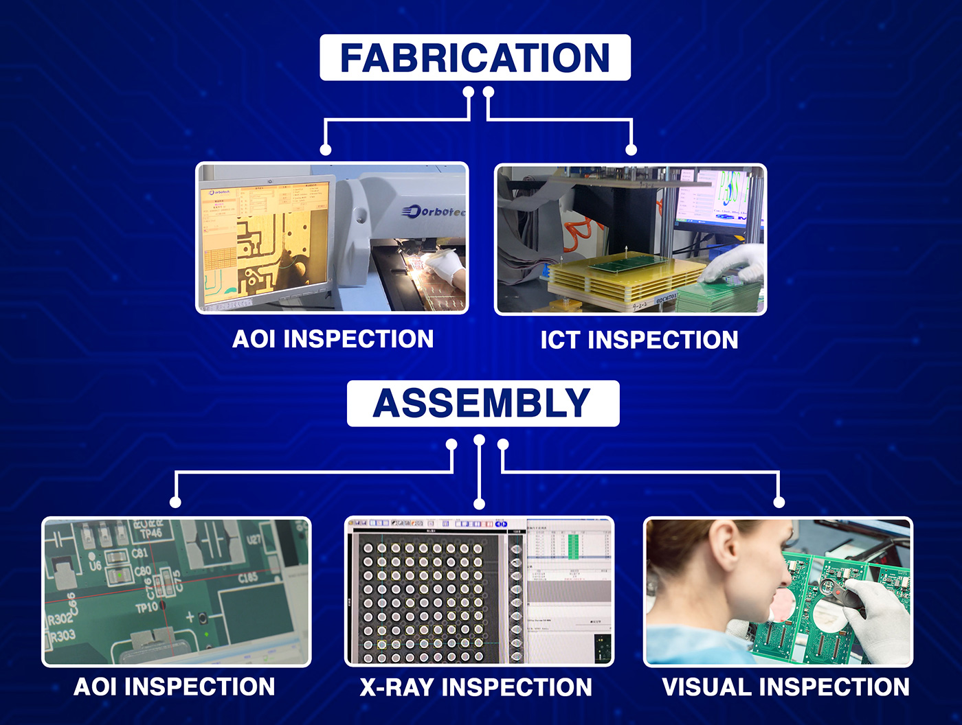
In the electronics industry, it is essential to carefully examine and identify defects before launching a product to consumers. Multiple inspection techniques are used in various steps of product development. Being a PCB manufacturer, Blind Buried Circuits understands that PCBs are an essential part of modern electronics. Product quality inspection must be performed on various stages to make the Printed Circuit Boards error-free. Depending on the complexity of the circuitry, product development engineers require various inspection and testing procedures to ensure the product is safe to use. To decide which inspection or testing techniques your design require, we have listed techniques to help you instruct your Electronic Manufacturer for your upcoming designs.
Visual Inspection:
The name says it all, although humans can make mistakes, research has shown that humans are better at making complex decisions than machines. But both have advantages and disadvantages, so after Automatic Optical Inspection, all the printed circuit boards are inspected by QA engineers who perform a visual quality inspection. Suppose you use discrete components like 01005, 0201, and 0402 packages. In that case, asking your Electronic Manufacturer to perform a visual inspection right after the printed circuit board assembly is recommended.
Automated Optical Inspection (AOI)
Automated Optical Inspection is used in various steps in PCB manufacturing and assembly. At the time of printed circuit board manufacturing, manually measuring the drill holes takes time for manufacturers to inspect whether the drills are drilled as per the provided diameters or not. Electronic Manufacturers like Blind Buried Circuits ensure that automated optical inspections compare each drill hole with the design files, which helps in manufacturing the printed circuit boards on a quick turn. In drilling and various manufacturing processes, there are conditions in which human involvement is not possible due to hazardous processes. Due to this, the manufacturers make sure that AOI takes place, and after the process completion, QA engineers visually inspect and generate the final inspection report.
With the help of cameras and image processing algorithms, it generates detailed inspection reports, which can be requested from your electronic manufacturer at the time of shipment.
While in the assembly process, AOI machines perform roles like inspecting component soldering, including the quality and cosmetically.
X-ray Inspection
With the help of X-radiations or X-rays, doctors can now easily inspect internal damages which are not visible by emitting electromagnetic radiation on the human body. But how come electronic manufacturer need x-ray technology for the inspection process while there are various inspection processes, such as AOI, which automatically detect the errors?
The question is valid till there was no inception of multilayer or HDI printed circuit boards. After stacking the layers, the manufacturers cannot separate the internal layers for inspection purposes. Due to this, X-Ray inspection ensures all the internal layers are connected, and there is no miss alignment in the drills while stacking up the copper layers.
Not only in PCB manufacturing but in PCB assembly, there are complex Ball Grid Array (BGA) surface mount packages that have a grid of small solder balls on the bottom and cannot be inspected visually due to which X-ray inspection takes place when there are BGA components on the printed circuit board. To check if BGAs are perfectly aligned, electronic manufacturers share the X-Ray inspection report with the customer when requested.
In-Circuit Testing (ICT)
Most designers nowadays prefer performing all types of testing, including functional testing, to ensure that the PCBs work properly without functional issues and no delay occurs in mass production. To ensure that, electronic manufacturer suggest In-Circuit testing or ICT testing, which takes place during the assembly process before it gets fully assembled. The testing procedure includes test probes with a bed of nails which tests each component’s values and verifies the functionality. This helps identify open, short, and incorrect parts values while assembling.
As ICT testing is a special testing requirement, your electronic manufacturer may require the following files before assembly:
Schematic diagram.
A complete Bill Of Material (BOM) file including quantities, reference designators, description, and manufacturing part numbers.
The original design files or CAD data can be generated from design software such as Altium or Eagle.
Gerber or ODB ++ files may vary depending on the manufacturer, as some work on Gerber 274x format, or some might work on ODB++ files.
Netlist files are generated from the design software to ensure that all the electrical connections between the components are maintained and that no shorts or broken nets are present in the design.
Testing software program files created based on the netlist and CAD data helps in programming the ICT machine and performing actual testing.
Flying Probe Testing
When it comes to cost-effectiveness, In-Circuit Testing (ICT) is considered expensive, due to which most of the electronic manufacturers like Blind Buried Circuits suggest flying probe testing for small and medium volume orders. The flying probe testing doesn’t require any type of custom fixture like the bed of nails, and it is performed by robotic probes, which move over the test points to ensure the values are correct based on the design data. The probes move and perform contact with test points and components in the specific location. First, the boards are loaded into the flying probe testing machine and positioned in a way that helps the probe to access the test points. Then after successful placement, the machine generates the TP or test point locations from design files.
Once all the locations get in contact with the probe, the FPT machine generates the test results and flags all the discrepancies if identified while comparing the collected data with design values. In case of any discrepancies, the designers can make changes in their next revision to avoid those issues in mass production.
Boundary Scan Testing
Boundary Scan Testing operates on a dedicated test infrastructure called Joint Test Action Group (JTAG) builtin into the ICs, which are placed on the PCBs and help to perform programming and testing of the devices. It is considered a fast and efficient option for complex digital circuits. It also doesn’t require any custom test fixtures or probes.
The test operates by JTAG testing software which incorporates the design of the PCB. The software generates a test program based on the JTAG infrastructure and device behavior. With the help of the JTAG interface, the program gets executed onto the device, which performs a series of internal registers and pins measurements. After the analysis process, the interface generates the report, which flags the discrepancies between the design files and the device.
Conclusion:
The electronic manufacturers perform inspection and testing based on the design and volume requirement. Furthermore, with the help of an inspection report, the designers can make necessary changes to their designs to avoid any issues in mass production. To make the product free of defects, there are multiple testing solutions such as visual inspection, automated optical inspection (AOI), X-ray inspection, in-circuit testing (ICT), flying probe testing, and Boundary Scan Testing.