

Objective
This blog explains why power integrity in PCB design matters, how it affects modern electronic
systems, and how engineers measure and address power delivery issues. It also covers the
relationship between power integrity and signal integrity, common PI challenges, practical
solutions, applications, and key benefits.
Key Takeaways
● Power integrity helps maintain stable voltage and current delivery across a PCB.
● A well-designed PDN helps control voltage droop, ripple, resonance, and supply noise.
● PI and signal integrity interact closely in high-speed PCB designs.
● Proper stackup, decoupling, vias, simulation, and manufacturing control can improve PI.
● Good PI supports reliable performance, signal margins, and efficient product
development.
Table Of Contents
- Introduction
- What Is Power Integrity (PI) in PCB Design?
- Where Power Integrity and Signal Integrity Meet?
- Why Is PI Important in PCB Design?
- How Do You Measure PI in PCB Design?
- Understanding PDN Impedance, Inductance, and Capacitance
- How Do PCB Stackup and Materials Affect PI?
- What Are the Common PI Challenges?
- How Can You Improve PI in PCB Design?
- Applications of PI in PCB Design
- Benefits of Good PI
- Why Choose Blind Buried Circuits for PCB Design?
- Frequently Asked Questions
Introduction
A printed circuit board (PCB) can meet its functional requirements and still develop voltage droop, ground bounce, supply ripple, or PDN resonance under real operating conditions. For
high-speed electronics, even a small disturbance can affect timing, data accuracy, EMI/EMC
performance, and overall system reliability.
This post explains why power integrity in PCB design matters and how it influences the
performance of modern electronic systems. It looks at how engineers identify and address power delivery issues before they become costly design or manufacturing problems, while also showing why PI and signal integrity for high-speed design need to be considered together.
What Is Power Integrity (PI) in PCB Design?
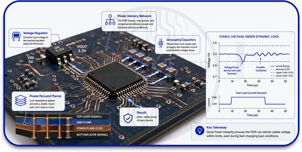
PI describes how effectively a PCB delivers stable voltage and transient current to its devices. The power delivery network (PDN) includes voltage regulators, copper planes, traces, vias, connectors, and decoupling capacitors.
A well-designed PDN keeps voltage within the limits required by each device as load conditions change. On a high-speed board, current demand can change within nanoseconds. If the PDN cannot respond quickly enough, voltage may dip or oscillate.
-
Where Power Integrity and Signal Integrity Meet?
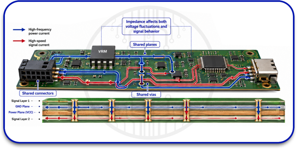
PI and SI interact through shared current paths, reference structures, and electromagnetic coupling. The interaction becomes increasingly significant as signal edge rates increase and supply voltage margins decrease.
-
-
- Current-path interaction: High-frequency currents associated with power delivery and signal transitions can share planes, vias, connectors, and other conductive structures. The impedance of these structures’ influences both voltage fluctuations and signal behavior.
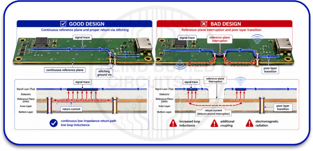
- Return-path continuity: A high-speed signal requires a continuous, low-impedance
return path. Reference-plane interruptions or poorly designed layer transitions can
increase loop inductance, causing additional coupling and electromagnetic radiation.
- Return-path continuity: A high-speed signal requires a continuous, low-impedance
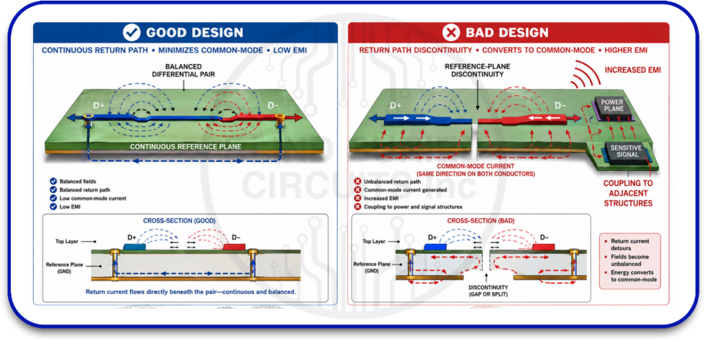
- Common-mode conversion: Discontinuities in differential-signal return paths can
convert differential energy into common-mode current. This can increase EMI and couple unwanted energy into adjacent power and signal structures.
- Common-mode conversion: Discontinuities in differential-signal return paths can
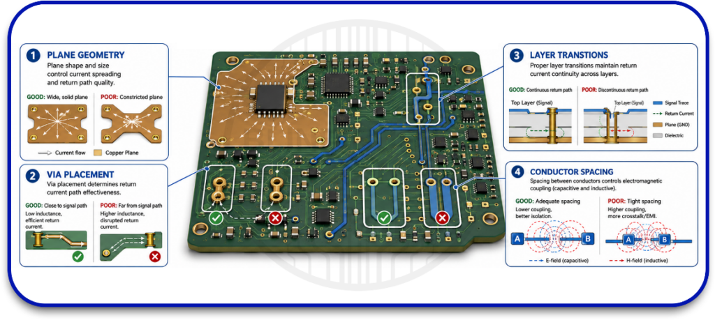
- Physical design: Plane geometry, via placement, layer transitions, and conductor spacing determine current distribution and electromagnetic coupling. These parameters should be evaluated for both PI and SI performance rather than optimized independently.
- Integrated verification: Correlate PDN impedance and transient response with
controlled impedance, return-path continuity, and coupling analysis during simulation and validation. This provides a more complete assessment of high-speed board behavior.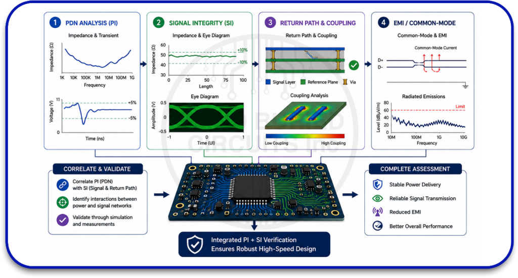
- Integrated verification: Correlate PDN impedance and transient response with
-
For OEMs, integrating PI and SI analysis during stackup development, layout, and verification
helps identify interactions that may remain hidden when each domain is assessed independently.Why Is PI Important in PCB Design?
Here is why PI is critical for maintaining voltage stability, signal margins, EMI/EMC
performance, and reliable operation in high-speed electronic systems.-
-
- Voltage stability: A transient load passing through PDN impedance produces voltage variation at the device supply pins. Higher PDN impedance can therefore increase rail noise and voltage droop.
- Signal margins: Supply disturbances can introduce power-supply-induced jitter and
reduce the voltage and timing margins available to high-speed interfaces. - EMI/EMC performance: High-impedance regions and resonant structures within a
PDN can generate unwanted electromagnetic emissions and contribute to EMC problems. - Thermal performance: Excessive current density increases resistive losses and Joule heating in conductors, which can affect electrical and thermal performance.
- System reliability: Maintaining supply voltage within device tolerances helps prevent
supply-related instability during dynamic operating conditions and high-current switching events.
-
How Do You Measure PI in PCB Design?
Here are the key methods used by engineers to measure and evaluate power integrity in PCB
design, with each providing insight into different aspects of PDN performance.-
-
- Time-domain measurement: An oscilloscope is used to measure supply ripple, voltage droop, overshoot, and transient response at critical IC supply pins. Excessive voltage variation during rapid load changes can then be identified. Low-inductance probing is required to minimize measurement-induced ringing.
- Frequency-domain analysis: A vector network analyzer is used to measure PDN
impedance across the relevant frequency range. Impedance peaks and resonant
frequencies that may increase supply noise can then be identified. For very low PDN
impedance, a calibrated method such as two-port shunt-through measurement is typically used. - Simulation-based analysis: PDN simulation is used to estimate impedance and transient response before fabrication. Potential issues involving capacitor networks, current paths, planes, vias, and package parasitics can therefore be identified while design changes remain practical.
● DC IR drop analysis: DC analysis is used to calculate resistive voltage loss across
traces, planes, vias, and other conductive paths. Voltage compliance at individual devices can then be verified under expected current loads.
-
These methods complement signal integrity in PCB design testing. Eye diagrams can evaluate timing and voltage margins, while TDR can locate impedance discontinuities.
Understanding PDN Impedance, Inductance, and Capacitance
PDN impedance, inductance, and capacitance determine how effectively a power delivery
network responds to changes in load current. Their interaction becomes particularly important at
higher frequencies, where parasitic effects can dominate nominal component values.-
-
- PDN impedance: PDN impedance represents the voltage variation produced by a change in load current across a given frequency range. A suitable target impedance should therefore be established from the allowable supply-voltage variation and expected transient current. Impedance should remain sufficiently low across the frequencies relevant to the device.
- Inductance: Inductance opposes rapid changes in current and becomes increasingly
significant as frequency rises. Vias, plane transitions, narrow connections, extended
current paths, and capacitor mounting structures can add parasitic inductance. These elements should be minimized where high-frequency transient current is required. - Capacitance: Capacitance provides charge during transient load events and contributes to lowering PDN impedance over selected frequency ranges. Different capacitor technologies and values may be required because their effective impedance is influenced by capacitance, equivalent series resistance, and equivalent series inductance.
- Capacitor placement: A decoupling capacitor is effective only when its electrical
connection to the load has sufficiently low impedance. Excessive connection length, via inductance, or an unsuitable mounting structure can reduce its high-frequency
effectiveness despite an adequate nominal capacitance value.
-
The key consideration is the complete electrical path between the voltage source, decoupling
network, and load. PDN performance should therefore be evaluated through impedance analysis, transient simulation, and measurement rather than by capacitor count alone.How Do PCB Stackup and Materials Affect PI?
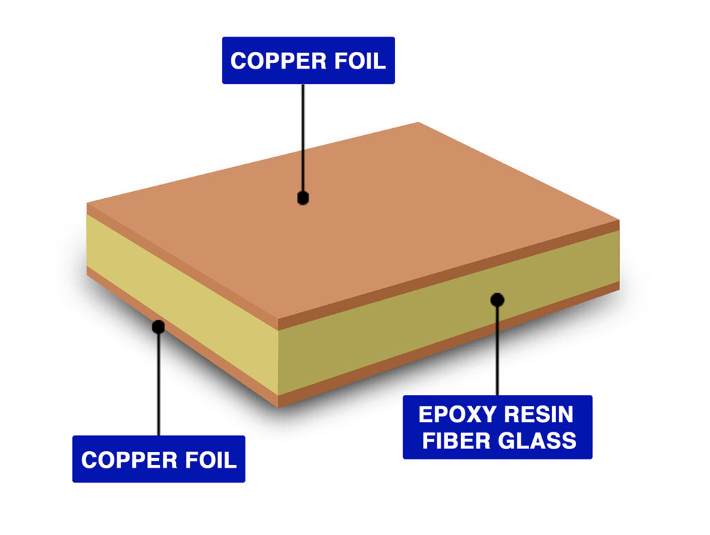
PCB stackup and material selection directly affect PDN impedance, plane capacitance, current paths, and high-speed signal performance.
-
-
- Power and ground plane coupling: Closely spaced power and ground planes reduce
loop inductance and increase the plane pair's distributed capacitance. This can lower PDN impedance over part of the frequency range. - Dielectric spacing: The distance between power and ground planes affects their
distributed capacitance. It also determines the geometry of transmission lines and
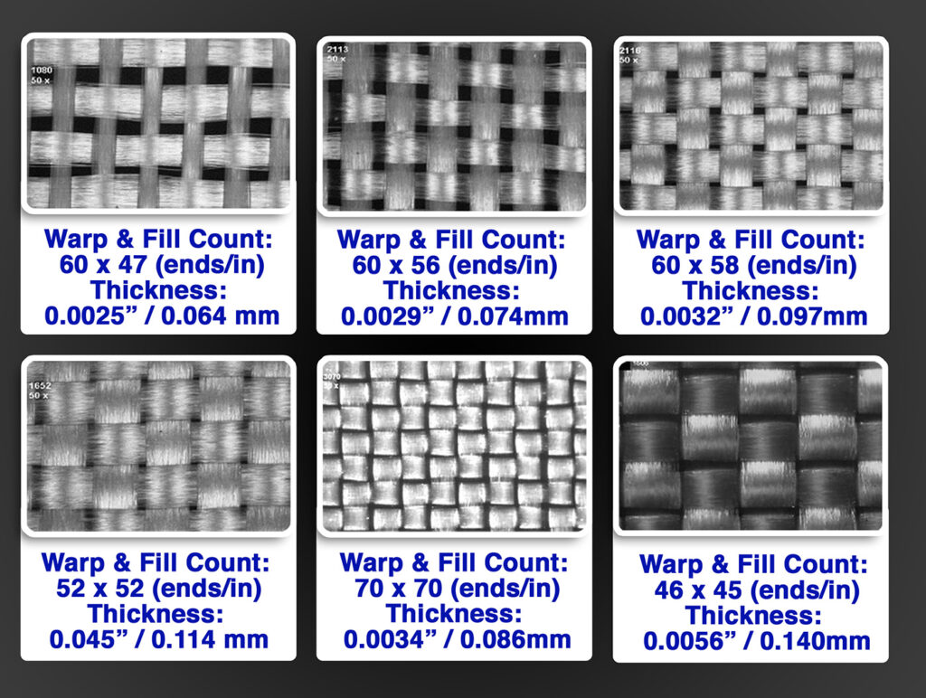
therefore influences controlled impedance. - Laminate selection: Dielectric constant affects transmission-line impedance and plane- pair capacitance, while dielectric loss and copper roughness affect high-frequency signal loss. Thermal and dimensional properties also affect fabrication and operating stability.
- Multilayer construction: Additional layers provide greater flexibility for separating
signal, power, and ground structures and for placing reference planes close to high speed signal layers. - HDI structures: Blind and buried vias, including microvias, provide interconnections
between selected layers without extending through the entire PCB. This can shorten
interconnects and preserve routing space in dense designs.
- Power and ground plane coupling: Closely spaced power and ground planes reduce
-
For dense high-speed PCBs, stackup selection should therefore be based on electrical
requirements, material properties, current distribution, and fabrication capabilities, rather than layer count alone.What Are the Common PI Challenges?
Several factors can degrade PDN performance. Early identification allows corrective changes to be made before fabrication.
-
-
- Voltage droop and ground bounce: Rapid changes in load current can produce voltage deviations across PDN resistance and inductance, causing local supply and ground potentials to vary.
- PDN resonance: Power and ground structures, capacitors, and parasitic inductances can form resonant networks, producing impedance peaks at specific frequencies.
- Decoupling placement: The parasitic inductance of capacitor connections can limit their effectiveness at higher frequencies, even when the nominal capacitance is appropriate.
- Via and plane discontinuities: Narrow current paths, excessive via inductance, or
interrupted planes can increase PDN impedance and alter return-current paths. - Thermal and current-density limits: High current density increases resistive loss and Joule heating in conductors, which can contribute to voltage drop and thermal stress.
- Power-to-signal coupling: Switching currents can couple through shared structures,
parasitic capacitance, or electromagnetic fields and introduce noise into sensitive signal paths.
-
These effects are interdependent. Changes to the stackup, via structure, capacitor placement, or current path can alter both PI performance and Signal Integrity in PCB Design.
How Can You Improve PI in PCB Design?
PI improvement begins with stackup definition and continues through layout, simulation, and
manufacturing.-
-
- Optimize decoupling: Place capacitors close to IC supply connections and select
suitable values based on the required frequency range, capacitance, ESR, and ESL. - Optimize vias: Use via-in-pad where appropriate to reduce connection inductance and add stitching vias to maintain low-inductance return paths between reference planes.
- Control impedance: Maintain the specified trace geometry, dielectric thickness, copper characteristics, and reference-plane configuration required for Signal Integrity High- Speed Design.
- Simulate before fabrication: Model PDN and signal behavior, compare stackup and
capacitor configurations, and resolve identified issues before design release. - Control manufacturing variation: Account for dielectric thickness, copper thickness,
via dimensions, and other relevant tolerances so fabricated electrical characteristics
remain within the specified design limits.
- Optimize decoupling: Place capacitors close to IC supply connections and select
-
Applications of PI in PCB Design
Power integrity is important in PCB designs where stable power delivery and low noise are
critical.-
-
- High-speed digital systems: Used in servers, processors, FPGAs, and networking
equipment to control supply noise during fast load changes. - RF and high-frequency boards: Helps reduce supply noise and unwanted coupling in
RF transceivers, amplifiers, and wireless systems. - Medical devices: Helps maintain clean power for sensitive analog and digital circuits used in imaging, monitoring, and diagnostic equipment.
- Automotive electronics: Supports stable power delivery in ECUs, sensors, cameras,
and ADAS systems under changing load conditions. - Industrial equipment: Helps control voltage variation and power noise in automation, motor-control, and communication systems.
- High-speed digital systems: Used in servers, processors, FPGAs, and networking
-
Benefits of Good PI
Effective PI contributes to both electrical performance and overall product development
outcomes.-
-
- Reduced EMI/EMC risk: A well-controlled PDN can help limit unwanted emissions
caused by supply noise, resonant behavior, and uncontrolled current paths, improving the likelihood of compliance-test success. - Improved signal margins: Stable supply voltage helps maintain timing, voltage, and
noise margins in high-speed interfaces, supporting more predictable Signal Integrity in PCB Design performance. - Higher system reliability: Consistent power delivery reduces the risk of intermittent
faults, unexpected resets, and supply-related instability under changing load conditions. - Fewer design revisions: Early PI analysis can identify PDN-related issues before
fabrication, reducing the likelihood of costly PCB re-spins and design modifications. - Improved development efficiency: Resolving PI concerns during design and validation can shorten debugging cycles, streamline testing, and help engineering teams maintain project schedules.
- Reduced EMI/EMC risk: A well-controlled PDN can help limit unwanted emissions
-
For OEMs developing high-speed, RF, automotive, medical, or industrial electronics, good PI
supports more predictable electrical performance throughout the product lifecycle.Why Choose Blind Buried Circuits for PCB Design?
For OEMs developing dense multilayer and HDI boards, fabrication capability must support the electrical requirements established during design. Blind Buried Circuits manufactures rigid, HDI, flex, rigid-flex, and multilayer PCBs, with capabilities including multilayer construction up to 50 layers, blind and buried vias, stacked and staggered microvias, and controlled impedance fabrication. We also support complex stackups and impedance-controlled designs using a range of standard and specialized laminate materials.
-