

Request our manufacturing capability
Capabilities
Low Volume PCB Assembly
Our Capabilities
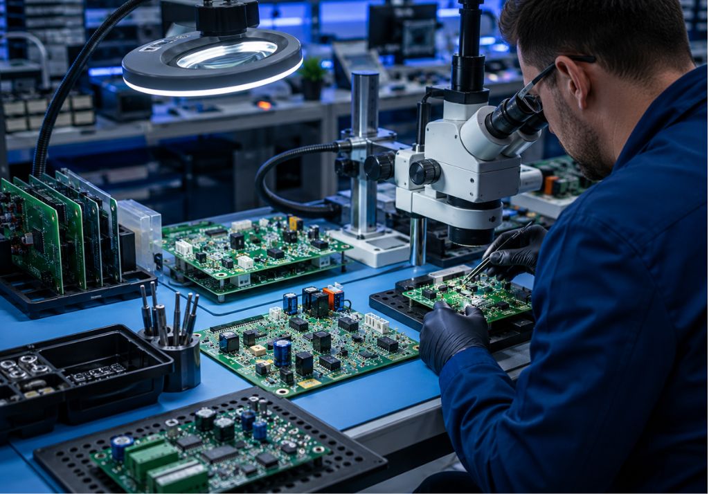
Low volume PCB assembly involves manufacturing and assembling printed circuit boards in small quantities, from a few prototypes to several hundred units, instead of moving directly into full-scale production. It is ideal for R&D, custom projects, pilot runs, niche electronic products, and New Product Introduction (NPI), where speed, flexibility, reliability, and cost control are critical. At Blind Buried Circuits, we offer low volume PCB assembly in the USA with quick-turn production, flexible order quantities, transparent pricing, DFM and DFT reviews, component mounting, inspection, and testing. Our small volume PCB assembly services help designers, OEMs, and product teams validate designs, make improvements quickly, and move efficiently from prototype development to market-ready products while maintaining consistent build quality.
Low Volume PCB Assembly Services Offered by Blind Buried Circuits
As a trusted low volume PCB assembly manufacturer, we combine engineering expertise, flexible production capabilities, and stringent quality standards to deliver reliable PCB assemblies tailored to your project requirements. We offer:
- Prototype PCB Assembly: We accelerate product development with rapid prototype PCB assembly for design validation, functional testing, and engineering revisions. Our quick-turn capabilities help reduce development cycles while maintaining the quality needed for a smooth transition to production.
- Engineering Support (DFM & DFT): Our engineering team provides Design for Manufacturing (DFM) and Design for Testing (DFT) support to optimize your PCB design for efficient manufacturing, reliable testing, and improved production yields before assembly begins.
- Complete Turnkey PCB Assembly: We simplify manufacturing by managing PCB fabrication, component sourcing, assembly, inspection, and final delivery through a single point of contact, reducing lead times and supply chain complexity.
- High-Mix, Low-Volume Production: We specialize in high-mix, low-volume manufacturing, supporting multiple PCB designs, product variants, and engineering revisions in flexible production quantities. This service is ideal for OEMs developing diverse or evolving electronic products.
- Component Procurement: Our procurement team sources quality electronic components from trusted suppliers, helping reduce sourcing challenges, improve component availability, and streamline your low volume PCB assembly projects.
- Advanced PCB Assembly: We support advanced PCB assembly for complex electronic designs, including surface mount technology, through-hole, mixed-technology, BGA, micro BGA, QFN, and other fine-pitch components. Our precision assembly process ensures reliable performance for high-density and multilayer PCB applications.
Low Volume PCB Assembly Process/ Workflow
Every low volume PCB assembly project at Blind Buried Circuits follows a structured manufacturing workflow designed to ensure quality, reliability, and repeatability. Here are the critical steps involved in our small volume PCB assembly services.
- Design Intake & DFM Review: The process begins with the submission of Gerber or ODB++ files, the Bill of Materials (BOM), stack-up details, impedance requirements, and other design specifications. Our engineers perform a comprehensive Design for Manufacturing (DFM) review to identify issues such as trace clearances, via-in-pad structures, flex bend zones, and thermal reliefs before production begins.
- Material Selection & Stack-Up Confirmation: Based on your project requirements, we select suitable substrate materials, including FR-4, Rogers, or polyimide, along with the appropriate copper weights, dielectric thicknesses, and layer stack-up.
- Lamination & Core Preparation: PCB cores and prepregs are prepared before undergoing high-pressure, high-temperature lamination. This process securely bonds the board layers while maintaining structural integrity and planarity for subsequent manufacturing stages.
- Drilling & Microvia Formation: Based on the PCB design requirements, mechanical or laser drilling is used to create through-holes, blind vias, buried vias, and microvias. The drilling method is selected according to the required hole size, layer structure, and HDI design requirements to ensure precise interlayer connectivity.
- Metallization & Copper Plating: After drilling, the holes and vias are metallized and copper plated to establish reliable electrical connections between PCB layers. Controlled plating ensures uniform copper deposition, improves via integrity, and enhances the long-term electrical and mechanical reliability of the finished PCB.
- Copper Patterning & Etching: Using customer-supplied design data, copper circuitry is patterned and etched to produce accurate traces, planes, differential pairs, and other critical circuit features while meeting specified trace and spacing requirements.
- Surface Finish, Solder Mask & Legend Printing: The finished PCB receives the required surface finish, including HASL, ENIG, ENEPIG, immersion silver, or OSP. Solder mask and legend printing are then applied to protect the circuitry, improve assembly accuracy, and enhance board identification.
- Component Assembly & Soldering: Electronic components are assembled using surface mount technology, through-hole, or mixed-technology processes. Our low volume PCB assembly capabilities support BGA, micro-BGA, QFN, and other fine-pitch components, followed by controlled reflow or wave soldering.
- Inspection & Testing: Each low volume PCB assembly undergoes comprehensive inspection and testing. Our testing capabilities include Solder Paste Inspection (SPI), Automated Optical Inspection (AOI), X-ray inspection for BGAs and buried vias, flying-probe electrical testing, impedance control and verification, and Functional Circuit Testing (FCT).
Advantages of Low Volume PCB Assembly
Low volume PCB assembly is more than just producing smaller quantities; it provides the flexibility, speed, and control needed to streamline product development and reduce manufacturing risks. Key advantages include:
- Faster Product Development: Small production runs enable rapid prototyping, design validation, and engineering revisions, helping reduce development time and speed up product commercialization.
- Lower Upfront Manufacturing Costs: Producing only the required quantity minimizes initial investment, making low volume PCB assembly a cost-effective solution for prototypes, pilot production, and specialized products.
- Greater Design Flexibility: Engineering changes can be implemented quickly without the expense of modifying high-volume production, allowing products to evolve throughout the development cycle.
- Reduced Inventory Risk: Manufacturing in smaller batches helps reduce excess inventory, lower storage costs, and minimize the risk of obsolete stock caused by design updates or changing market demand.
- Faster Time to Market: Quick-turn manufacturing and flexible production schedules enable companies to respond faster to customer requirements and market opportunities.
- Easy Transition to Production: Once a design has been validated, the same manufacturing processes can be scaled efficiently from prototype and pilot builds to higher production volumes, reducing risk during product launch.
Applications & Industries We Serve
As a trusted low volume PCB assembly manufacturer, Blind Buried Circuits delivers reliable low volume PCB assembly solutions for the following industries that require precision, flexibility, and fast turnaround.
- Aerospace & Defense: We support prototype development and low-volume production of avionics, communication systems, and other mission-critical electronics that require precision, reliability, and consistent performance.
- Automotive & Electric Vehicles (EV): Our low volume PCB assembly services help automotive manufacturers develop and validate battery management systems (BMS), motor controllers, sensors, and power electronics before full-scale production.
- Telecommunications & 5G: We manufacture low volume PCB assemblies for RF modules, networking equipment, and 5G communication systems, enabling faster product validation and engineering revisions.
- Medical Devices & Healthcare Electronics: We build reliable PCB assemblies for diagnostic equipment, patient monitoring systems, wearable devices, and other medical electronics requiring precision manufacturing and quality assurance.
- Industrial Electronics & Automation: Our low volume PCB assembly solutions support industrial automation systems, robotics, instrumentation, and embedded control devices through prototype and pilot production.
- Renewable Energy & Power Electronics: We support the development of renewable energy systems, battery storage solutions, and power conversion equipment through flexible low volume PCB assembly services.
- Semiconductor & High-Tech Systems: We manufacture precision PCB assemblies for semiconductor equipment, evaluation boards, breakout boards, and other advanced electronic systems requiring rapid engineering validation.
- Research & New Product Introduction (NPI): Our low volume PCB assembly services help engineering teams validate new designs, conduct functional testing, and transition efficiently from prototype development to pilot production
Quality & Compliance
Every low volume PCB assembly project at Blind Buried Circuits is supported by stringent quality management processes to ensure reliable performance, manufacturing consistency, and compliance with recognized industry standards, including:
- IPC-6012 Class II for general electronic products.
- IPC-6012 Class III for high-reliability and mission-critical applications.
- IPC-2223 design guidelines for rigid-flex PCB designs, where applicable.
- IPC-4101 and IPC-4204 requirements for substrate and laminate materials to ensure reliable dielectric and thermal performance.
Start Your Low Volume PCB Assembly Project with Blind Buried Circuits
As a trusted low volume PCB assembly in the USA, we combine engineering expertise, flexible manufacturing, and rigorous quality standards to help you move confidently from design to production. Ready to get started? Contact our team today to discuss your requirements or request a customized quote for your low volume PCB assembly project.
Frequently Asked Questions
We routinely support 4 mil trace and 4 mil space for rigid PCBs, along with laser-drilled microvias for HDI designs. Via-in-pad technology with filling and plating is also available, depending on your design requirements.
Yes. Our low volume PCB assembly services support lead-free manufacturing using RoHS- and REACH-compliant solder alloys and optimized thermal profiles to meet industry and environmental standards.
For single-layer polyimide flex sections, the recommended minimum bend radius is typically 5× the flex thickness after assembly. We also recommend defining bend zones in the Gerber files for evaluation during the DFM review.
Yes. We support Rogers and other high-frequency laminate materials with controlled impedance, optimized dielectric thickness, and carefully engineered stack-ups for RF and high-speed electronic applications.
We use sequential lamination, precision drilling, and controlled copper plating to ensure reliable interlayer connections for HDI PCBs. Every assembly is verified using X-ray inspection, flying-probe electrical testing, or Functional Circuit Testing (FCT) to confirm connectivity and long-term reliability.
Yes. We offer quick-turn low volume PCB assembly services for prototype and pilot production projects, with delivery available in as little as 3–5 working days for eligible designs, subject to material and component availability.







Ready To Get Started?
To learn more about our PCB Design Guidelines, don’t hesitate to contact our sales team at sales@blindburiedcircuits.com.