


Objective
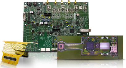
This blog explains what printed circuit board defects are, why they occur, and which defects are most common during PCB manufacturing and assembly. You’ll also learn where defects can develop during production, how DFM helps prevent them, and how proper inspection and manufacturing controls improve PCB quality and long-term reliability.
Key Takeaways
- Printed Circuit Board Defects can occur during design, fabrication, assembly, or testing.
- Common PCB defects include open circuits, shorts, plating issues, layer misregistration, solder mask problems, and surface finish defects.
- Proper DFM review helps identify manufacturing risks before production begins.
- PCB inspection and testing help detect defects before boards move to assembly or final products.
- Controlling fabrication and assembly processes improves PCB reliability and reduces rework and scrap.
- Working with an experienced PCB manufacturer helps maintain consistent quality from prototype through production.
Table Of Contents
- What Are Printed Circuit Board Defects?
- Why Do PCB Manufacturing Defects Occur?
- What Are the Most Common PCB Manufacturing Defects?
- Where Do PCB Defects Occur During Manufacturing?
- How Does DFM Help Reduce PCB Manufacturing Defects?
- How Do PCB Defects Affect Assembly and Long-Term Reliability?
- How Does Blind Buried Circuits Maintain PCB Quality?
- Why Choose Blind Buried Circuits?
- Frequently Asked Questions
What Are Printed Circuit Board Defects?
Printed Circuit Board Defects are manufacturing or assembly problems that cause a PCB to differ from its required design, electrical, dimensional, or quality specifications.
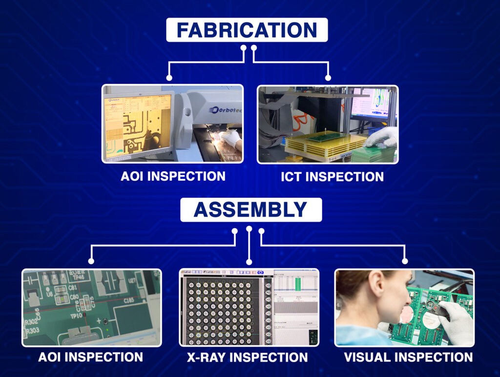
Some defects can be identified through visual inspection, while others require electrical testing, automated optical inspection (AOI), X-ray inspection, or other testing methods.
PCB defects can occur at different stages, including:
- PCB design and layout
- Material preparation
- Imaging and etching
- Drilling
- Copper plating
- Lamination
- Solder mask application
- Surface finishing
- PCB assembly
- Inspection and testing
Identifying defects early is important because a small fabrication problem can become a larger assembly or reliability issue later in the manufacturing process.
Why Do PCB Manufacturing Defects Occur?
PCB Manufacturing Defects can result from design limitations, material issues, process variations, equipment conditions, or inadequate inspection.
For example, a PCB design may use very tight trace spacing or a small annular ring. If these features do not match the manufacturer’s capabilities, the risk of fabrication problems can increase.
Common causes include:
- Incorrect trace width or spacing
- Improper hole sizes and tolerances
- Insufficient annular ring
- Incorrect PCB material selection
- Drilling inaccuracies
- Uneven copper plating
- Over-etching or under-etching
- Layer misregistration
- Lamination problems
- Solder mask misregistration
- Surface finish issues
- Poor solder paste or reflow control
This is why PCB quality should be considered from the design stage through final inspection rather than only after the board has been manufactured.
What Are the Most Common PCB Manufacturing Defects?
The following PCB Defects List covers some of the Common PCB Defects that can occur during PCB fabrication and assembly.
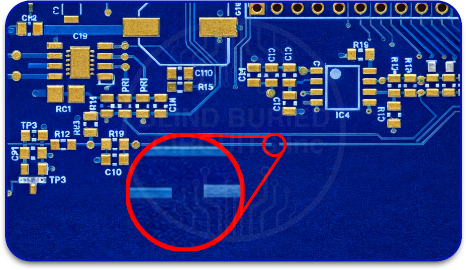
1. Open Circuits: An open circuit occurs when a copper path is broken, preventing the intended electrical connection between two points on the PCB.
Common Causes:
● Excessive etching of copper traces
● Insufficient copper plating
● Mechanical damage during handling or processing
● Poor connections between PCB layers
Prevention:
● Maintain appropriate trace widths during PCB design
● Control etching parameters during fabrication
● Maintain consistent copper plating thickness
● Use electrical testing to verify circuit continuity
2. Short Circuits: A short circuit occurs when two conductive features that should remain electrically separated make unintended contact.
Common Causes:
● Insufficient trace or pad spacing
● Etching problems
● Copper residue between conductors
● Solder mask registration issues
Prevention:
● Perform DFM checks for spacing requirements
● Maintain accurate imaging and etching processes
● Verify solder mask registration
● Use AOI and electrical testing to identify shorts

3. Delamination: Delamination occurs when layers within a PCB separate because of insufficient bonding or excessive thermal or mechanical stress.
Common Causes:
● Incorrect lamination temperature or pressure
● Moisture in laminate materials
● Contamination between layers
● Improper material selection
Prevention:
● Control lamination temperature, pressure, and cycle time
● Store PCB materials under recommended conditions
● Prevent contamination during fabrication
● Select laminate materials suitable for the application

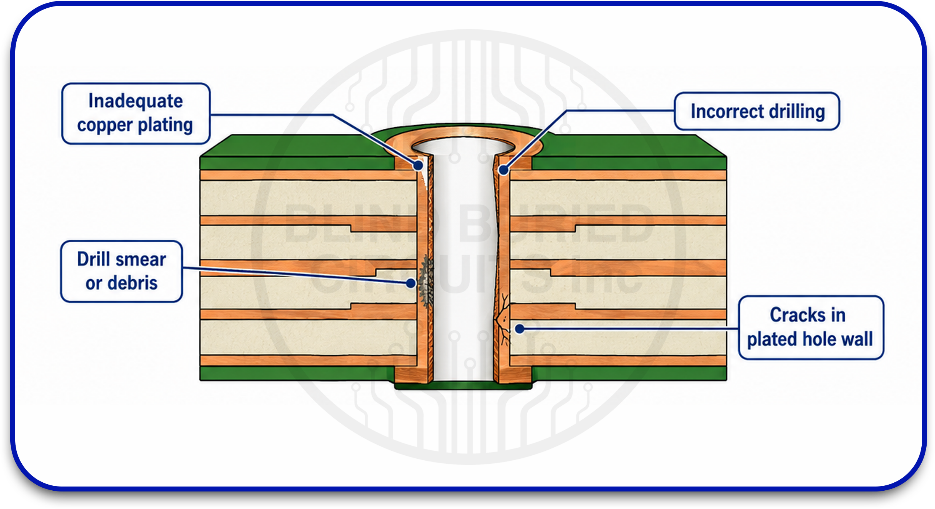
4. Via and Plated Hole Defects: Via and plated hole defects occur when a hole does not provide a reliable electrical or mechanical connection between PCB layers.
Common Causes:
● Inadequate copper plating
● Incorrect drilling parameters
● Drill smear or debris
● Cracks in the plated hole wall
Prevention:
● Optimize drilling parameters for the selected material
● Maintain consistent desmear and plating processes
● Inspect plated holes during fabrication
● Use cross-section analysis when required
5. Solder Mask Misalignment: Solder mask misalignment occurs when the solder mask opening does not properly align with the intended pad or copper feature.
Common Causes:
● Artwork or imaging registration errors
● PCB material movement during processing
● Incorrect exposure or alignment
● Process variation
Prevention:
● Maintain accurate imaging and exposure settings
● Control registration throughout fabrication
● Verify solder mask alignment during inspection
● Follow appropriate pad and solder mask clearances during PCB design
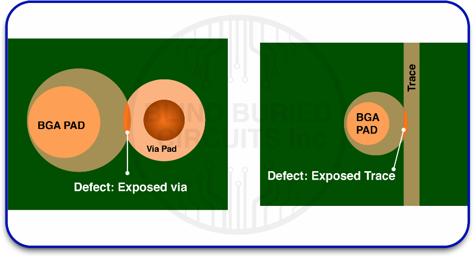
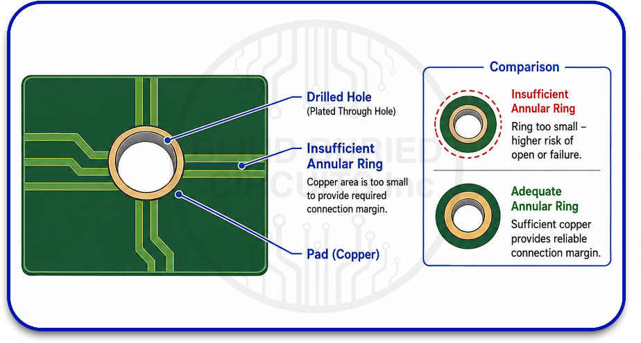
6. Insufficient Annular Ring: An insufficient annular ring occurs when the copper area surrounding a drilled hole is too small to provide the required connection margin.
Common Causes:
● Small pad dimensions
● Drill-position variation
● Incorrect hole-to-pad design
● Layer registration issues
Prevention:
● Allow adequate annular ring during PCB layout
● Verify hole and pad tolerances during DFM
● Maintain accurate drilling and registration processes
● Inspect critical hole features during fabrication
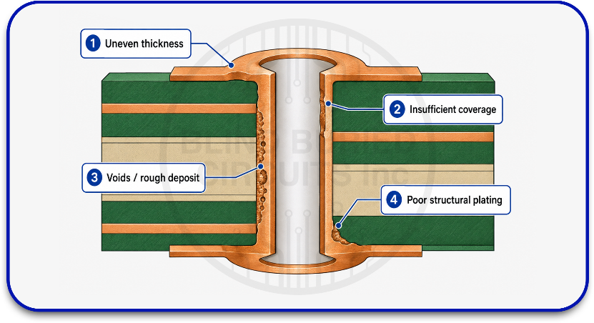
7. Copper Plating Defects: Copper plating defects occur when the deposited copper does not meet the required thickness, coverage, or structural requirements.
Common Causes:
● Unstable plating conditions
● Poor surface preparation
● Inadequate current distribution
● Contamination
Prevention:
● Control plating chemistry and process parameters
● Maintain proper surface preparation
● Monitor copper thickness
● Perform appropriate inspection and testing
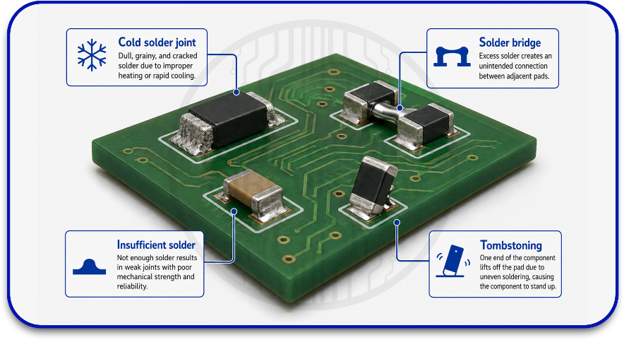
8. PCB Soldering Defects: PCB Soldering Defects occur during assembly when solder does not form the
intended reliable connection between a component and its PCB pad.
Common Causes:
● Incorrect solder paste volume
● Improper stencil design
● Incorrect reflow profile
● Component or pad misalignment
● PCB surface finish problems
Prevention:
● Optimize stencil aperture design
● Control solder paste application
● Verify the reflow profile
● Maintain accurate component placement
● Inspect solder joints using appropriate inspection methods
Where Do PCB Defects Occur During Manufacturing?
PCB defects can occur at different stages of the manufacturing process. Understanding where they develop makes it easier to apply the right preventive controls.
| Manufacturing Stage | Common Defects |
| PCB Design | Incorrect spacing, trace width, hole size, and annular ring |
| Material Preparation | Moisture, contamination, or material issues |
| Imaging & Etching | Over-etching, under-etching, and trace-width variation |
| Drilling | Hole-size variation, misregistration, and breakout |
| Plating | Insufficient copper, cracks, and uneven plating |
| Lamination | Delamination and layer misregistration |
| Solder Mask | Pinholes, peeling, and mask misregistration |
| Surface Finish | Poor coverage, oxidation, and solderability issues |
| PCB Assembly | Solder bridges, insufficient solder, and tombstoning |
| Testing | Electrical or workmanship defects identified during inspection |
How Does DFM Help Reduce PCB Manufacturing Defects?
Design for Manufacturing (DFM) helps determine whether a PCB design can be manufactured consistently using the manufacturer’s available processes and capabilities.
A DFM review can identify potential problems before fabrication begins.
Important DFM checks include:
- Trace width and spacing
- Hole sizes and tolerances
- Annular ring
- Copper-to-edge clearance
- Via design
- Layer stackup
- Solder mask clearance
- Surface finish
- Material selection
- Manufacturing tolerances
For complex multilayer and high-density boards, DFM is especially important because small design tolerances can create manufacturing challenges.
A proper DFM review helps engineers identify potential issues while changes are still easy to make, reducing the risk of rework, scrap, and production delays.
How Do PCB Defects Affect Assembly and Long-Term Reliability?
Not every PCB defect causes an immediate failure. Some defects may pass initial testing but create problems during assembly or affect reliability over time.
For example, inadequate copper plating inside a via can weaken an electrical connection. A poor solder joint may also become unreliable after repeated thermal cycling.
PCB defects can lead to:
- Assembly problems
- Rework and scrap
- Intermittent electrical failures
- Reduced product reliability
- Production delays
- Field failures
- Increased manufacturing costs
For high-reliability applications, controlling PCB fabrication and assembly processes from the beginning helps reduce the risk of defects and long-term failures.
How Does Blind Buried Circuits Maintain PCB Quality?
PCB quality starts with proper design review, controlled manufacturing processes, and appropriate inspection.
Blind Buried Circuits provides PCB manufacturing and assembly services with capabilities for different board technologies and production requirements.
Quality control can involve reviewing PCB designs, checking manufacturing requirements, inspecting fabricated boards, and performing appropriate electrical and assembly testing.
Blind Buried Circuits supports PCB requirements including:
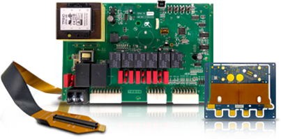
- Multilayer PCB Manufacturing
- HDI PCB Manufacturing
- Rigid PCB Manufacturing
- Flexible PCB Manufacturing
- Semi-Flex PCB Manufacturing
- Prototype PCB Services
- PCB Assembly Services
- Production-Volume PCB Manufacturing
A controlled manufacturing process helps identify potential problems early and reduces the chance of defects moving from fabrication into assembly or final production.
Why Choose Blind Buried Circuits?
Choosing a PCB manufacturing partner requires more than evaluating fabrication cost. The manufacturer should understand how PCB design, materials, fabrication, assembly, and testing work together.
Blind Buried Circuits supports customers with:
- PCB manufacturing and assembly
- Prototype and production support
- DFM and DFA analysis
- Multilayer PCB manufacturing
- HDI PCB capabilities
- Rigid and flexible PCB solutions
- Custom PCB manufacturing
- Quality-focused manufacturing processes
Whether you are developing a prototype or preparing for production, early communication with the manufacturer can help identify potential manufacturing issues before they affect the final product.