

Objective
This blog explains PCB panelization, its common methods, design guidelines, depanelization processes, and how proper panel design can improve PCB manufacturing efficiency.
Key Takeaways
- PCB panelization combines multiple PCBs into one larger panel for efficient manufacturing.
- Proper PCB panel design improves material utilization, handling, and production efficiency.
- V-scoring, tab routing, and other methods help secure PCBs within a panel.
- PCB panelization guidelines help ensure reliable assembly and depanelization.
- Proper depanelization reduces mechanical stress and board-edge damage.
Table Of Contents
- What Is PCB Panelization?
- How Does the PCB Panelization Process Work?
- Common PCB Panelization Methods
- What Is PCB Depanelization and What Are the Common Methods?
- Common PCB Panelization and Depanelization Challenges
- Benefits of PCB Panelization
- Why Choose Blind Buried Circuits for PCB Manufacturing?
- Frequently Asked Questions
What Is PCB Panelization?
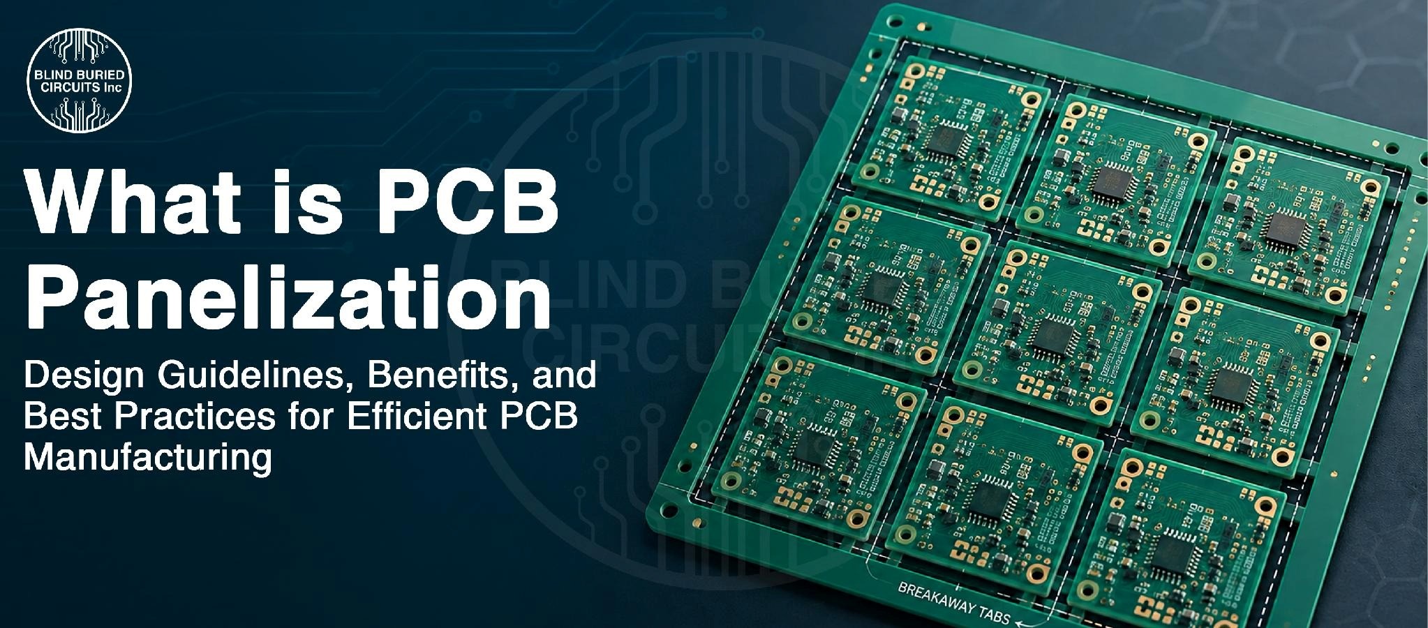
PCB panelization is the process of arranging multiple individual printed circuit boards into a single larger PCB panel for manufacturing and assembly. Instead of processing each board separately, manufacturers produce and handle the boards together as one panel and separate them after fabrication or assembly.
A properly designed panel helps maintain board stability, supports automated manufacturing processes, and makes better use of the available PCB material. The PCB panel design can include features such as panel rails, tooling holes, fiducials, and breakaway structures based on the requirements of fabrication and assembly.
The panelization approach depends on factors such as board size, shape, thickness, component placement, production volume, and the required depanelization method.
How Does the PCB Panelization Process Work?
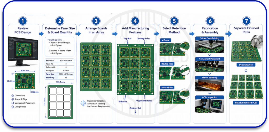
PCB panelization follows a structured process and it typically involves the following steps:
- Review of the Individual PCB Design: The process begins by evaluating the dimensions, shape, board thickness, component placement, and edge geometry of each PCB. These characteristics help determine how effectively the boards can be arranged within a larger panel.
- Determining Panel Dimensions and Board Quantity: The manufacturer establishes suitable PCB panel dimensions based on fabrication capabilities, assembly equipment, material utilization, and production requirements. The available panel area then helps determine how many individual boards can be accommodated.
- Arrangement of the Boards into an Array: Individual PCBs are positioned and oriented within the panel to make efficient use of the available material while creating a configuration suitable for downstream manufacturing and PCB assembly processes.
- Addition of Manufacturing Features: Panel rails, tooling holes, fiducials, and other process-specific features are incorporated into the PCB panel design. These features support panel alignment, handling, registration, and accurate processing through automated equipment.
- Selection of the Board-Retention Method: An appropriate method is selected to keep the individual PCBs securely connected throughout manufacturing. Depending on the board geometry and production requirements, this may involve V-scoring, routed tabs, mouse bites, or a combination of methods.
- Fabrication and Assembly of the Panel: The complete panel is fabricated as a single unit and can proceed through assembly operations such as solder paste printing, component placement, reflow soldering, inspection, and testing without handling each PCB individually.
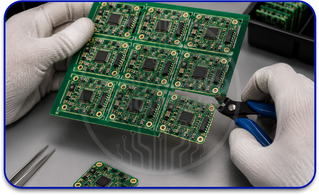
- Separation of the Finished PCBs: Once fabrication and assembly are complete, the individual boards are removed from the panel using the selected depanelization process. The method used for depaneling PCB assemblies should provide clean separation while minimizing mechanical stress and the risk of damage to components, solder joints, and board edges.
Common PCB Panelization Methods
The method used to secure individual boards within a PCB panel depends on board geometry, component placement, manufacturing requirements, and the intended depanelization process. Common PCB panelization methods include:
- V-Scoring: V-scoring forms opposing V-shaped grooves along predetermined straight lines in the PCB panel, leaving a controlled thickness of material between them. It is well suited to rectangular boards arranged in rows or columns and can support efficient panel utilization. However, score lines typically run continuously from one panel edge to another, limiting their suitability for irregular board outlines.
- Tab Routing: Tab routing uses a router to cut around most of the PCB outline while leaving small tabs that hold the board within the panel. It accommodates irregular shapes and complex board profiles more effectively than V-scoring. However, sufficient spacing is required between boards to accommodate the router bit.
- Mouse-Bite Tabs: Mouse bites are commonly incorporated into routed tabs rather than used as a separate routing method. A series of small holes drilled through the tab creates a weakened section that allows easier depaneling PCB assemblies. This approach works well for complex board outlines but can leave small protrusions along the separated edge.
- Solid Tabs: Solid tabs are unperforated sections of material left during routing to hold individual boards within the panel. They provide strong mechanical support during manufacturing but require cutting, routing, or another controlled process for separation.
- Combination Panelization: A PCB panel design may combine V-scoring and tab routing when board geometry or layout makes a single approach impractical. For example, straight edges may use V-scores while other areas use routed tabs. This provides greater layout flexibility while maintaining the mechanical support required during manufacturing.
- PCB Panelization Design Guidelines :Although exact requirements vary by manufacturer and assembly process, the following PCB panelization guidelines should be considered during panel development:
- Maintain Board-to-Board Spacing: Provide sufficient spacing between individual PCBs based on the selected panelization and depanelization method. Routed panels require clearance for the router bit, while V-scored boards can generally be positioned closer together.
- Provide PCB-to-Panel-Edge Clearance: Maintain adequate clearance between the outermost PCBs and panel edges to accommodate panel rails, tooling features, handling requirements, and assembly equipment.
- Allow Component-to-Edge Clearance: Keep components, particularly large or mechanically sensitive ones, sufficiently away from board edges, V-score lines, and breakaway tabs to reduce the risk of mechanical stress or damage during depanelization.
- Include Panel Rails: Add rails or borders where required to improve panel rigidity and provide suitable handling areas for conveyors, fixtures, and automated assembly equipment.
- Position Tooling Holes Appropriately: Place tooling holes to support accurate and repeatable panel positioning in manufacturing equipment and fixtures. Their size and location should meet the requirements of the fabrication and assembly processes.
- Use Fiducial Marks: Include global fiducials to help automated assembly equipment identify the position and orientation of the overall PCB panel. Local fiducials may also be required near fine-pitch or high-accuracy components to improve placement accuracy.
- Plan Breakaway Tabs Carefully: Position breakaway tabs to provide adequate mechanical support during processing while minimizing stress on the PCB and nearby components during separation.
- Maintain Copper-to-Edge Clearance: Keep traces, copper pours, planes, and other conductive features at an appropriate distance from routed edges and V-score lines to prevent copper exposure or damage during fabrication and depanelization.
- Maintain Panel Rigidity: Ensure the panel remains sufficiently rigid during solder paste printing, component placement, reflow, inspection, and handling. Board arrangement, panel rails, tab placement, material thickness, and large routed openings can all affect mechanical stability.
What Is PCB Depanelization and What Are the Common Methods?
PCB depanelization is the process of separating individual circuit boards from a larger PCB panel after fabrication or assembly. The separation method is typically considered during PCB panel design as board geometry, retention features, component placement, production volume, and required edge quality influence the appropriate technique.
Careful depaneling of PCB assemblies is especially important when components, solder joints, or other sensitive features are located near board edges. Excessive mechanical force during separation can introduce stress or damage.
Common depanelization methods include:
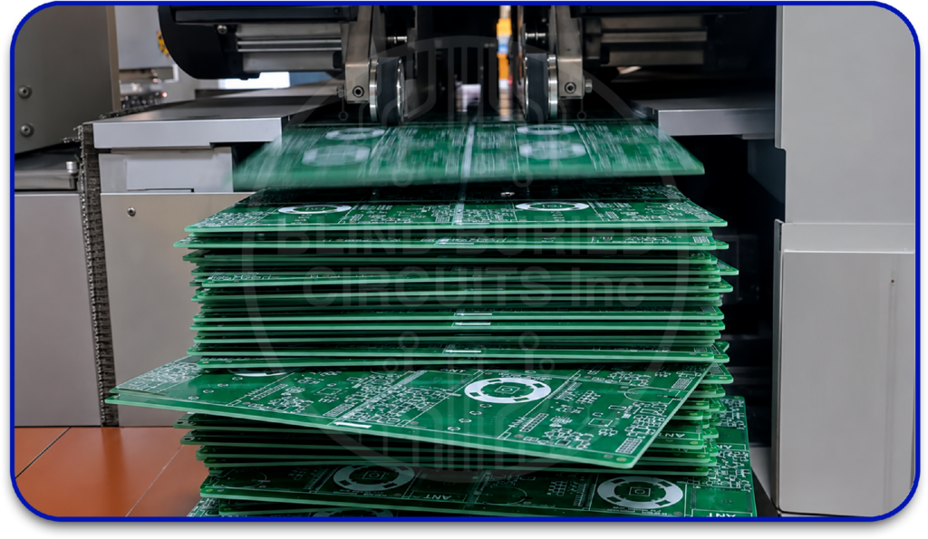
V-Score Depanelization: V-score depanelization separates boards along pre-scored grooves using controlled mechanical force. It is efficient for rectangular PCBs with straight separation lines and is well suited to high-volume production.
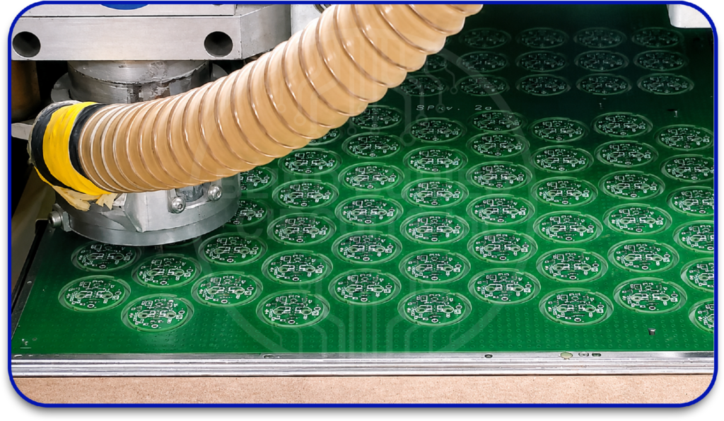
Routing or Milling: Routing uses a rotating cutting tool to separate boards along a defined profile. It accommodates irregular shapes and complex outlines while providing controlled separation and clean board edges.
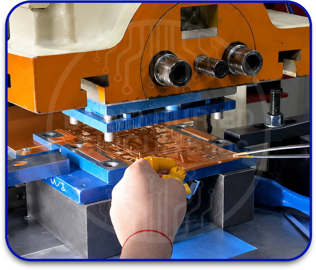
Punching: Punching uses a dedicated die to separate PCBs from the panel in a fast, repeatable operation. It is suitable for high-volume production but requires custom tooling, making it less practical for low-volume or frequently changing designs.
Manual Depanelization: Manual depanelization separates boards by hand or with hand-operated tools. It can be practical for prototypes and low-volume production, provided the panel design allows separation without excessive bending or mechanical stress.
Common PCB Panelization and Depanelization Challenges
Effective PCB panelization requires balancing material efficiency, panel stability, assembly requirements, and reliable board separation. Several challenges can arise when these factors are not properly coordinated:
- Optimizing Material Utilization: Arranging boards efficiently can be challenging, particularly with irregular PCB shapes or mixed designs. Poor nesting can reduce board yield per manufacturing panel and increase material waste.
- Controlling Panel Bow and Warpage: Thin materials, uneven copper distribution, thermal exposure, and extensive routed areas can affect panel flatness, potentially interfering with assembly, soldering, handling, and inspection.
- Balancing Clearance and Panel Utilization: Providing adequate clearance for components, routing paths, V-scores, and breakaway features while maximizing the number of boards per panel can be challenging, particularly for compact or densely populated PCB designs.
- Managing Panel Stability: Extensive routing, large cutouts, thin board constructions, or insufficient support can reduce PCB panel rigidity, making reliable handling and processing through assembly equipment more difficult.
- Controlling Depanelization Stress: Mechanical separation can introduce bending, twisting, vibration, or cutting forces that may stress solder joints, components, traces, or the PCB substrate.
- Maintaining Board-Edge Quality: Depaneling PCB assemblies can leave rough edges, tab remnants, or other edge defects if the separation method and process are not properly controlled.
- Panelizing Irregular PCB Shapes: Curved, angled, or complex PCB profiles can make pose challenges in efficient panelization as it may require routing, additional spacing, or specialized panel arrangements.
Benefits of PCB Panelization
- Better Material Utilization: Maximizes the use of PCB material and reduces waste.
- Faster Production: Allows multiple boards to be processed together.
- Simplified Assembly: Supports efficient automated printing, placement, and inspection.
- Lower Manufacturing Costs: Reduces handling time and improves production efficiency.
- Improved Panel Stability: Provides better support during fabrication and assembly.
- Consistent Processing: Helps maintain uniform manufacturing and assembly conditions across multiple PCB boards.
Why Choose Blind Buried Circuits for PCB Manufacturing?
Blind Buried Circuits integrates PCB panelization into the manufacturing process, helping customers move from individual board designs to production-ready panels with efficient coordination between fabrication and assembly. Our experience with rigid, flex, rigid-flex, HDI, and blind and buried via technologies enables us to accommodate both standard and complex panelization requirements.
Ready to move your PCB design into production? Send us your design files and production requirements today to discuss your PCB manufacturing and panelization needs