

Objective
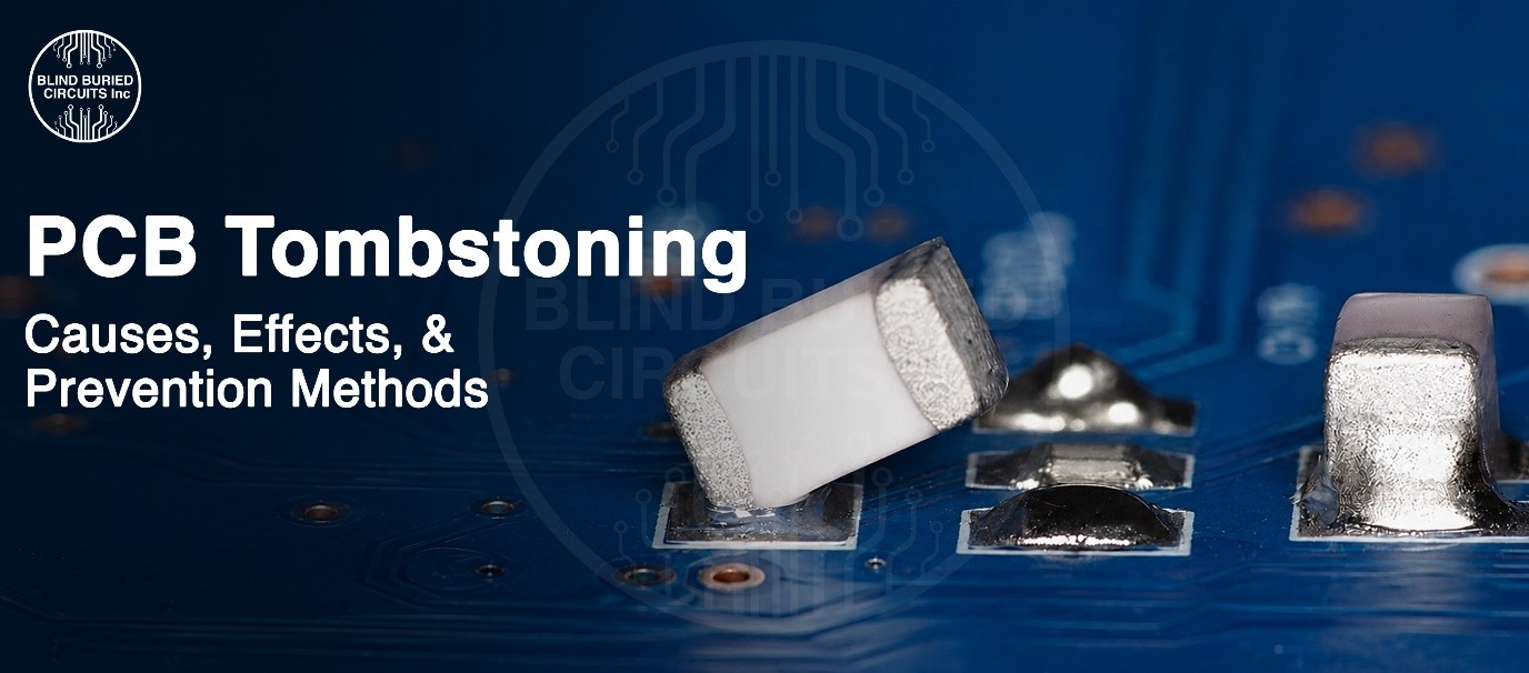
PCB tombstoning is one of the most common defects encountered during Surface Mount Technology (SMT) assembly. Although it may appear to be a minor issue, it can lead to open circuits, product failures, lower manufacturing yields, and increased production costs.
This article explains what Tombstoning PCB Assembly is, why it occurs, its effects on PCB performance, and the best practices manufacturers can follow to prevent it. Whether you’re a PCB designer, electronics engineer, or contract manufacturer, understanding tombstoning can help improve assembly quality and product reliability.
Key Takeaways
- PCB tombstoning occurs when one end of a surface-mount component lifts off the PCB during reflow soldering.
- Uneven solder wetting, poor pad design, incorrect solder paste volume, and improper reflow profiles are the most common causes.
- Even small process variations can lead to tombstone defects, especially in miniature SMT components.
- Proper PCB design, stencil optimization, and controlled SMT processes significantly reduce the risk of tombstoning.
- Regular inspection and process validation help improve manufacturing yield and long-term PCB reliability.
Table of Contents
- What Is PCB Tombstoning?
- Why PCB Tombstoning Is a Critical SMT Assembly Issue
- Common Causes of PCB Tombstoning
- PCB Design and Manufacturing Factors That Increase Tombstoning
- Effects of PCB Tombstoning on PCB Performance
- How to Detect Tombstone Defects in PCB Assembly
- Best Practices and Ways to Prevent PCB Tombstoning
- How Blind Buried Circuits Helps Minimize PCB Tombstoning
- FAQs
What Is Tombstoning in PCB?
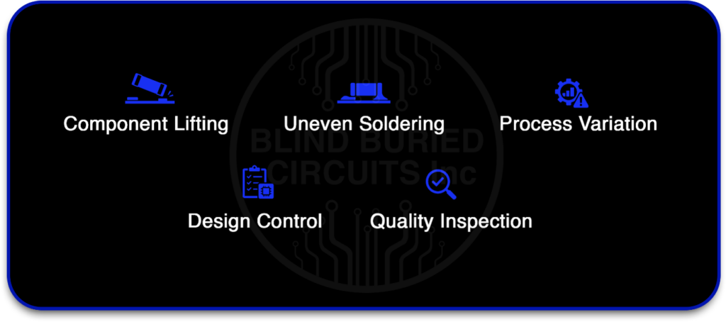
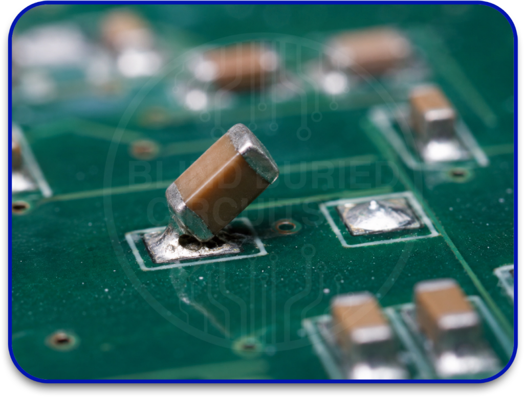
PCB tombstoning is a common Surface Mount Technology (SMT) assembly defect that primarily affects small passive components such as resistors, capacitors, and inductors. It occurs when one end of a component lifts from its solder pad during the reflow soldering process, resulting in an incomplete or open electrical connection. This tombstone defect in PCB assembly is caused by an imbalance in solder wetting forces.
The PCB tombstone effect can reduce product reliability, increase manufacturing defects, and lead to costly rework if not identified and corrected during PCB assembly.
Key characteristics include:
- One end of the component lifts from the PCB pad during reflow soldering.
- Uneven solder wetting forces create an imbalance that causes the component to stand upright.
- Small passive components such as 0201, 0402, and 0603 packages are more susceptible to tombstoning
Why PCB Tombstoning Is a Critical SMT Assembly Issue
Modern electronic devices require reliable solder joints to ensure consistent performance. Tombstoning PCB Assembly can interrupt electrical connections, reduce manufacturing yield, and increase production costs. Identifying and preventing this defect early helps improve product quality and assembly efficiency.
| Impact Area | How PCB Tombstoning Affects Assembly |
| Electrical Performance | Creates open circuits and unreliable connections. |
| Product Reliability | Increases the risk of product failure over time. |
| Manufacturing Yield | Raises defect rates and lowers first-pass yield. |
| Production Cost | Requires additional inspection, rework, or board replacement. |
| Quality Control | Delays production and affects overall assembly efficiency. |
Common Causes of PCB Tombstoning
PCB tombstoning is typically caused by a combination of design, material, and process-related factors rather than a single issue. The table below summarizes the most common causes.
| Cause | How It Contributes to PCB Tombstoning |
| Uneven Solder Paste Deposition | Unequal solder paste volume creates unbalanced surface tension, causing one end of the component to lift during reflow. |
| Poor PCB Pad Design | Unequal pad sizes, shapes, or land patterns create uneven heating and solder wetting. |
| Incorrect Component Placement | Misaligned components result in uneven solder wetting and increase the risk of the tombstone effect in PCB. |
| Improper Reflow Temperature Profile | Incorrect heating rates or temperature settings cause one solder joint to melt before the other. |
| Oxidized Pads or Component Leads | Poor solderability delays wetting on one side, creating unequal soldering forces. |
| PCB Surface Finish | Surface finishes with inconsistent solderability can affect wetting and contribute to PCB tombstoning. |
| Small Passive Components | Lightweight components such as 0201, 0402, and 0603 packages are more susceptible to lifting during reflow. |
| PCB Warpage or Thermal Imbalance | Board warpage and uneven copper distribution create temperature differences that can lead to tombstoning. |
PCB Design and Manufacturing Factors That Increase Tombstoning
Successful SMT assembly depends on maintaining a balanced soldering process from PCB design to final assembly. Even when components are placed accurately, certain design and manufacturing factors can increase the risk of Tombstoning PCB Assembly.
| Factor | Why It Matters |
| PCB Pad Design | Unequal pad sizes or shapes create uneven soldering forces. |
| Stencil Design | Incorrect aperture size can deposit too much or too little solder paste. |
| Copper Distribution | Uneven copper areas affect heat absorption during reflow. |
| Component Placement | Off-centre placement creates unbalanced surface tension. |
| Reflow Profile | Incorrect temperature settings lead to uneven solder melting. |
| PCB Surface Finish | Poor solderability delays wetting on one side of the component. |
Maintaining consistency across these factors helps reduce assembly defects and improves overall manufacturing quality.
Effects of PCB Tombstoning on PCB Performance
Although a tombstone defect in PCB may seem like a minor cosmetic issue, it can significantly affect product performance and reliability.
| Effect | Impact |
| Open Circuits | Interrupts electrical connections and prevents normal circuit operation. |
| Signal Integrity Issues | Causes unstable electrical performance in sensitive circuits. |
| Reduced Reliability | Weak solder joints are more likely to fail over time. |
| Increased Manufacturing Costs | Requires additional inspection, repair, or board replacement. |
| Lower Production Yield | More rejected boards reduce manufacturing efficiency. |
In High-Density PCB Assembly applications and high-reliability industries such as medical devices, aerospace, automotive, and industrial electronics, even a single tombstone defect can lead to costly failures.
How to Detect Tombstone Defects in PCB Assembly
Early detection is essential for reducing production costs and improving assembly quality. Manufacturers typically use multiple inspection methods to identify PCB tombstoning before products move to the next manufacturing stage.
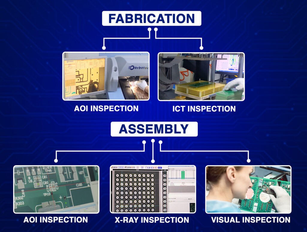
- Visual Inspection: Operators examine the PCB for components that appear tilted or standing vertically after reflow soldering.
- Automated Optical Inspection (AOI): AOI systems use high-resolution cameras to quickly detect missing, misaligned, or tombstoned components across the entire PCB.
- X-Ray Inspection: For complex or high-density assemblies, X-ray inspection helps identify hidden solder joint defects that cannot be seen during visual inspection.
- Functional Testing: Electrical testing confirms whether each component is properly connected and operating as intended before shipment.
Best Practices and Ways to Prevent PCB Tombstoning
Tombstoning in PCB is one of the most common SMT assembly defects, and applying the following best practices helps improve manufacturing quality and reliability
- Optimize PCB Pad Design: Design symmetrical pads that heat evenly and provide balanced solder wetting during reflow.
- Improve Stencil Printing: Use properly designed stencil apertures to ensure consistent solder paste volume on every pad.
- Ensure Accurate Component Placement: Calibrate pick-and-place equipment regularly to maintain precise component alignment.
- Optimize the Reflow Profile: Develop a controlled temperature profile that allows both solder joints to melt uniformly.
- Select High-Quality Materials: Use quality solder paste, PCB surface finishes, and components that provide consistent solderability.
- Follow Design for Manufacturability (DFM) Guidelines: Applying DFM principles during PCB layout helps identify potential manufacturing issues before production begins.
How Blind Buried Circuits Helps Minimize PCB Tombstoning
At Blind Buried Circuits, preventing PCB tombstoning starts with a quality-focused manufacturing process. Our engineering team performs Design for Manufacturability (DFM) reviews to optimize PCB layouts before production. During SMT assembly, we use precise solder paste printing, accurate component placement, and optimized reflow profiles to ensure reliable solder joints.
Every PCB assembly undergoes thorough quality inspections, including Automated Optical Inspection (AOI) and functional testing, to detect defects before shipment. By combining advanced manufacturing processes with strict quality control, our optimized manufacturing processes also help minimize the tombstone effect in PCB, ensuring consistent solder joint quality across complex PCB assemblies. Looking for reliable PCB Assembly Services?
Contact Blind Buried Circuits today to discuss your project and discover how our experienced engineering team helps minimize the PCB tombstone effect, improve manufacturing quality, and deliver reliable PCB assemblies.
Frequently Asked Questions
1. What is the main cause of PCB tombstoning?
Ans: The most common cause of a tombstone defect in PCB is uneven solder wetting during reflow soldering, often resulting from unequal solder paste deposition, thermal imbalance, or poor PCB pad design.
2. Which PCB components are most likely to experience tombstoning?
Ans: Small SMT passive components, including 0201, 0402, and 0603 resistors, capacitors, and inductors, are the most susceptible because they require very little force to lift during reflow.
3. Can PCB tombstoning be prevented completely?
Ans: While it cannot always be eliminated, PCB tombstoning can be significantly reduced through proper PCB design, optimized stencil printing, accurate component placement, and controlled reflow soldering.
4. How is PCB tombstoning detected during assembly?
Ans: Manufacturers typically detect PCB tombstoning using Automated Optical Inspection (AOI), visual inspection, X-ray inspection (when required), and functional testing.
5. Why is Design for Manufacturability (DFM) important for preventing PCB tombstoning?
Ans: A DFM review helps identify design issues such as uneven pad geometry, thermal imbalance, and improper land patterns before manufacturing, reducing the risk of tombstone defects.