

Objective
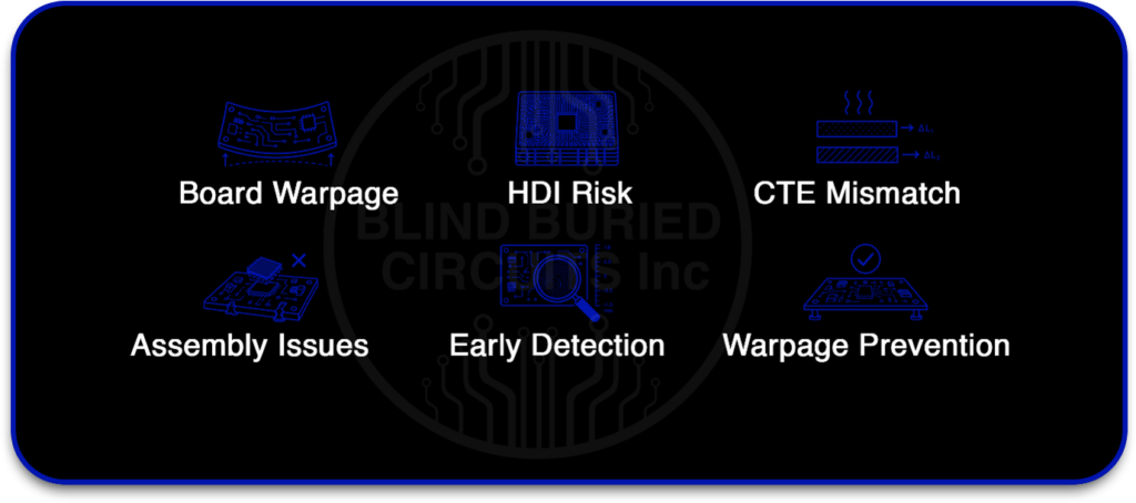
This article explains what PCB warpage is, the major PCB warpage causes across fabrication and assembly, how PCB warpage analysis is performed, and how board deformation affects PCB assembly reliability, manufacturing yield, and long-term product performance.
Key Takeaways
- PCB warpage refers to the bending, twisting, or distortion of a PCB from its flat shape
- Multilayer and HDI boards are more susceptible to PCB board warpage
- CTE mismatch and stack-up asymmetry are major PCB warpage causes
- PCB warpage can affect solder paste printing, BGA alignment, and reflow reliability
- PCB warpage analysis helps detect deformation before assembly defects occur
- Preventing warpage during PCB design and fabrication is more effective than post-assembly correction
Table of Contents
- Introduction
- What Is PCB Warpage
- Common PCB Warpage Causes
- How PCB Warpage Affects PCB Assembly
- PCB Warpage Analysis: Measurement Methods for Early Detection and Process Control
- Preventing PCB Warpage in Assembly: Design and Process Best Practices
- PCB Warpage in Blind and Buried Via Designs: Increased Stack-Up Sensitivity
- Why Blind Buried Circuits Is the Right Partner for Complex PCB Challenges
- Frequently Asked Questions
Introduction
As PCB designs become smaller, denser, and more complex, maintaining board flatness throughout fabrication and assembly has become increasingly challenging. Even minor deformation can create significant manufacturing issues, affecting solder joint quality, component alignment, assembly yield, and long-term reliability.
These challenges are especially common in multilayer PCBs, HDI designs, and high-temperature lead-free assembly processes where thermal and mechanical stresses are more pronounced. Without proper control, PCB warpage can lead to assembly defects, increased rework, and higher production costs.
PCB warpage is closely associated with bow and twist in PCB manufacturing. These two measurements are industry-standard methods used to evaluate the flatness of a printed circuit board. While PCB warpage describes the overall deformation, bow and twist PCB measurements help manufacturers determine whether the board falls within acceptable tolerances defined by industry standards. Understanding the relationship between PCB warpage and bow and twist is essential for ensuring high-quality PCB fabrication and assembly.
Whether you’re designing multilayer PCBs, High-Density Interconnect (HDI) boards, or high-reliability electronic assemblies, understanding the causes, effects, and prevention methods of PCB warpage is critical to improving manufacturing efficiency and product performance.
What Is PCB Warpage
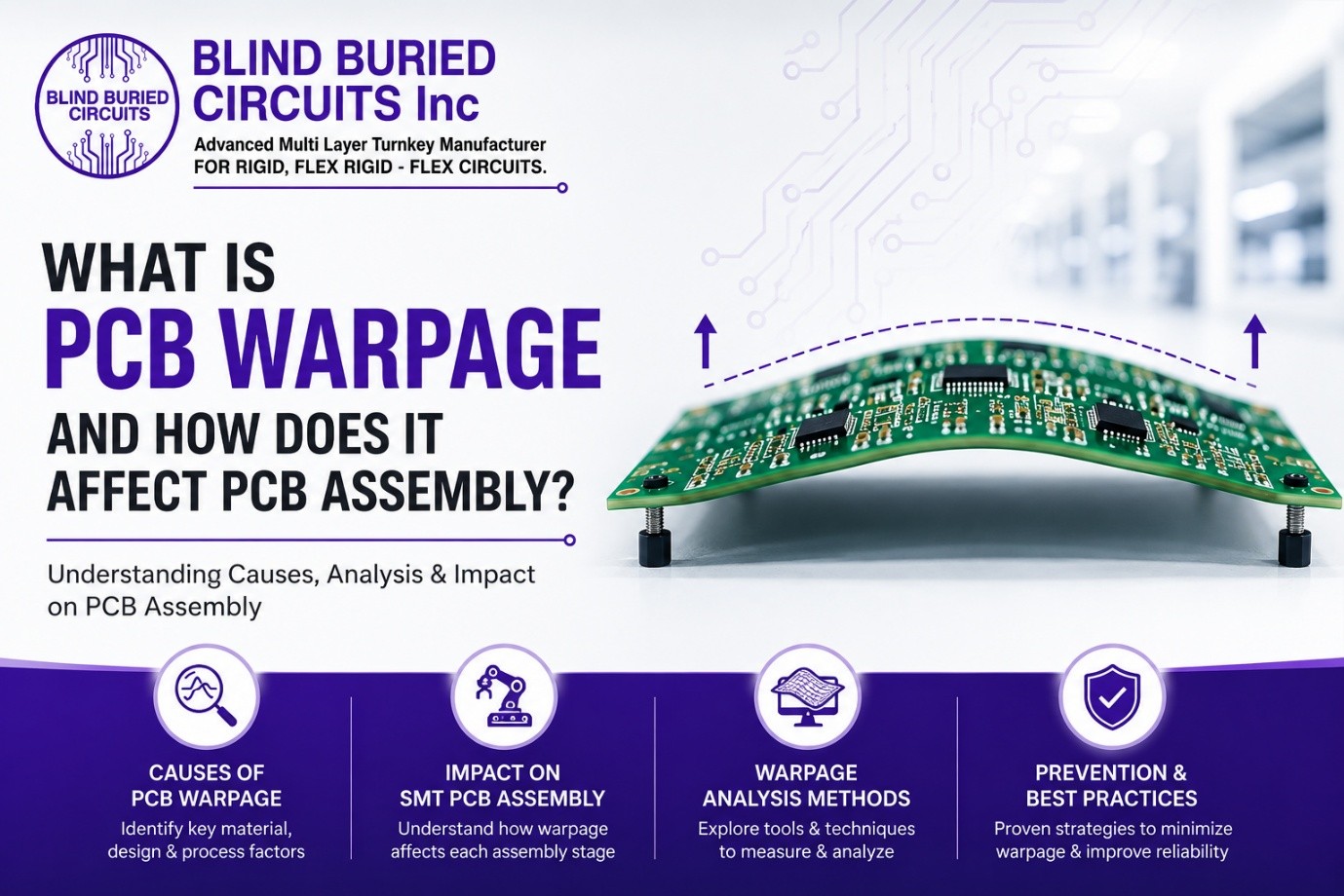
PCB warpage refers to the unintended bending, twisting, or distortion of a printed circuit board from its original flat shape. The deformation may occur during PCB fabrication, thermal processing, storage, transportation, or PCB assembly operations. In high-density electronic assemblies, even small variations in board flatness can affect manufacturing precision and electrical reliability.
Warpage in PCB manufacturing is generally measured in terms of bow and twist:
- Bow: Curvature along a single axis of the board
- Twist: Distortion where opposite corners are no longer aligned on the same plane
According to IPC standards, PCB flatness tolerance is typically measured as a percentage of board dimensions. The governing standard, IPC-TM-650, sets a maximum limit of 0.75% for SMT PCBs. Practically, this means a 300 mm board should deviate no more than 2.25 mm across its length. For high-density assemblies, particularly those involving fine-pitch BGAs, QFNs, or multilayer HDI boards, even that limit can be too generous. A working threshold of 0.5% is widely considered more appropriate for modern assembly environments. Excessive deviation beyond acceptable limits can interfere with automated assembly processes and solder joint formation.
PCB warpage becomes more prominent in:
- Multilayer PCBs
- HDI boards
- Thin-core PCB designs
- Large-format panels
- High-temperature lead-free assemblies
Some level of warpage is generally unavoidable in PCB manufacturing. The lamination and curing processes used in bare board fabrication naturally introduce internal mechanical stress. The objective, therefore, is not to eliminate warpage entirely, but to ensure it remains controlled and within acceptable engineering tolerances.
Common PCB Warpage Causes Across Fabrication and Assembly
PCB warpage rarely results from a single issue. Instead, it is usually caused by a combination of design decisions, material characteristics, and manufacturing processes that introduce internal stresses within the board.
The same factors responsible for PCB warpage also contribute to excessive bow and twist in PCB assemblies. By identifying and controlling these root causes, manufacturers can significantly reduce both warpage and bow-and-twist-related defects.
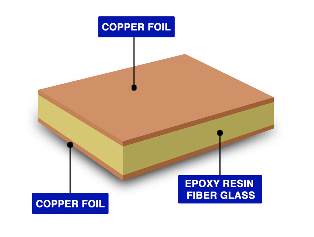
- CTE Mismatch and Material Incompatibility: Different materials such as copper, fiberglass, and resin expand at different rates during thermal cycling. This mismatch generates internal stress during soldering and reflow, causing the stack-up to bend toward the layer experiencing higher net shrinkage during cooling.
- Unbalanced Copper Distribution: Uneven copper density across layers leads to differential thermal expansion during heating and cooling cycles. High-density power or ground planes versus sparse signal layers create mechanical imbalance, making this a frequent driver of PCB warpage in complex multilayer designs.
- Stack-up Asymmetry: Non-symmetric stack-ups cause uneven mechanical response under thermal load. When material type, thickness, or dielectric properties differ across the center core, the board tends to curl toward the side with higher shrinkage during cooling.
- Thermal Process Variability During Assembly: Reflow and soldering introduce additional thermal stress even in initially flat boards. Non-uniform oven profiles, aggressive cooling rates, and mechanical fixturing constraints can induce out-of-plane deformation during thermal expansion and contraction cycles.
- Design-Related PCB Warpage Causes: PCB design decisions significantly influence mechanical stability. Compact layouts with uneven component distribution, dense BGA clustering, thin substrate selection, and large unsupported areas can introduce structural imbalance and localized stress during thermal cycling.
- Mechanical Handling and Manufacturing Errors: Improper handling during fabrication or assembly can permanently deform PCB structures. Excessive clamping force, inadequate fixturing, conveyor misalignment, and stress during depanelization all contribute to PCB board warpage even after successful fabrication.
How PCB Board Warpage Impacts PCB Assembly Processes
Even when a PCB meets electrical requirements, excessive board deformation can create challenges during assembly. Modern SMT processes rely on precise board flatness to ensure accurate solder paste deposition, component placement, and solder joint formation. As warpage increases, the risk of manufacturing defects and reliability concerns also rises.
- Solder Paste Printing: Stencil printing relies on a controlled and uniform stencil-to-PCB interface. PCB warpage disrupts this interface by creating variable contact pressure across the board surface. Areas of local bow or deflection result in inconsistent paste transfer, leading to non-uniform solder paste volumes. This condition increases the likelihood of insufficient solder, excess deposition, solder bridging, and open joints after reflow.
- Component Placement: Automated placement systems are referenced to a planar PCB datum. PCB board warpage introduces Z-axis variation across the assembly surface, affecting placement accuracy and component seating. Fine-pitch and area-array components, particularly BGAs, are sensitive to non-coplanarity, which may result in misalignment, poor solder ball contact, and latent interconnection defects such as head-in-pillow conditions.
- Reflow Soldering: During reflow, elevated temperatures reduce PCB stiffness and amplify existing warpage conditions. Out-of-plane deformation under thermal load and component weight can result in localized loss of contact in area-array devices. This may produce open solder joints, incomplete reflow, or non-wetting conditions that are not always detectable through post-process visual inspection.
- Downstream Quality, Yield, and Cost Impact: PCB warpage contributes to reduced first-pass yield, increased rework, and higher scrap rates. Certain defects may bypass visual and automated inspection processes, resulting in latent reliability failures. In high-reliability sectors such as automotive, aerospace, and medical electronics, such failures directly impact qualification compliance, field reliability, and overall cost of ownership.
PCB Warpage Analysis: Measurement Methods for Early Detection and Process Control
Early detection of PCB warpage is essential for maintaining assembly yield and preventing downstream defects. PCB warpage analysis at incoming inspection, prior to component placement, helps ensure compliance with flatness requirements and reduces the risk of assembly disruption. Three primary methods are in common use:
- Mechanical Gauging Methods: Mechanical gauges provide a cost-effective baseline method for measuring bow and twist along PCB edges. These tools are used for basic flatness verification against IPC-A-600 acceptance criteria and are typically applied during incoming inspection for standard assemblies.
- Laser Scanning and Shadow Moiré Techniques: Laser scanning and shadow moiré systems generate full-field, three-dimensional surface maps of the PCB. These methods provide high-accuracy warpage distribution data across the entire board area and are preferred for fine-pitch, HDI, and high-layer-count assemblies requiring detailed deformation analysis.
- Optical Profilometry: Optical profilometry is a non-contact structured light technique that delivers high-resolution surface topography data. It is applied where tight warpage tolerances are specified or when in-process measurement and validation of dimensional stability are required.
For critical assemblies, particularly those involving BGAs, multilayer HDI structures, or high-reliability end applications, PCB warpage analysis should extend beyond room-temperature inspection. Simulation of deformation behavior under reflow conditions using thermal moiré systems or finite element modeling during design provides a more accurate representation of in-process board behavior rather than static as-received conditions.
Preventing PCB Warpage in Assembly: Design and Process Best Practices
Prevention of PCB warpage is more effective than post-process correction. Once a PCB or assembled PCB exceeds flatness tolerances, corrective actions are limited, and mechanical intervention may introduce additional risks such as solder joint microcracking or latent reliability defects. Warpage control must therefore be addressed across design, fabrication, and assembly stages.
- At the Design Stage: Symmetric stack-up construction should be maintained, with layer arrangement mirrored around the central core to minimize internal stress imbalance. Copper distribution across opposing layers should be balanced, typically within a 10 percent variation. Panel rails and outrigger areas should be designed with copper density comparable to the active PCB region. Material selection should ensure compatible CTE and Tg values across the stack-up, using fabricator-qualified laminate sets where possible.
- During Fabrication: Pre-baking of bare PCBs prior to assembly may be used to reduce absorbed moisture and relieve residual laminate stress. Controlled lamination pressure profiles and defined cooling rates are required to minimize internal stress retention. Process consistency during multilayer pressing is critical to maintaining dimensional stability before the board reaches assembly.
- In the Assembly Process: Reflow fixtures should support the PCB adequately without restricting natural thermal expansion. Uniform mid-span support, controlled edge clearance, and low-force perimeter restraints help manage out-of-plane deformation during thermal cycling. Reflow profiles should be optimized to control peak temperature and dwell time while maintaining solder joint integrity. Rigid mechanical clamping during soldering should be avoided to prevent thermally induced warpage.
- For Procurement and Quality Teams: Incoming inspection of bare PCBs should be performed against IPC-TM-650 flatness criteria prior to release into production. Requirement of material certifications, stack-up details, and fabrication process documentation enables traceability and supports root-cause analysis in the event of warpage-related nonconformance.
PCB Warpage in Blind and Buried Via Designs: Increased Stack-Up Sensitivity
High-density interconnect (HDI) designs incorporating blind and buried vias introduce higher mechanical and thermal sensitivity during fabrication. Sequential lamination cycles required to build internal interconnect structures introduce repeated thermal excursions, increasing cumulative stress within the laminate system and elevating the risk of dimensional instability.
Each additional lamination cycle increases the likelihood of CTE-induced mismatch effects and stack-up imbalance. As process complexity increases, tighter control over material selection, copper distribution, and layer symmetry becomes essential to maintain PCB warpage within defined tolerances.
In these structures, PCB warpage is not a secondary manufacturing outcome but a direct function of stack-up design integrity. Effective control requires early-stage co-design between PCB designers and fabricators, ensuring that mechanical stability is addressed alongside electrical performance requirements.
Why Blind Buried Circuits Is the Right Partner for Complex PCB Challenges
Controlling PCB warpage requires more than meeting standard fabrication requirements. It demands careful attention to stack-up design, material selection, copper balancing, thermal processing, and assembly readiness. As PCB designs become more complex, manufacturers need a partner with the engineering expertise and process controls necessary to minimize deformation risks before they impact production.
At Blind Buried Circuits, we specialize in manufacturing advanced multilayer PCBs, HDI boards, and blind and buried via designs where dimensional stability is critical. Our engineering team collaborates with customers during the design phase to evaluate stack-up symmetry, material compatibility, copper distribution, and other factors that influence PCB warpage.
As a USA-based PCB manufacturer, we combine advanced manufacturing capabilities with rigorous quality-control processes, including in-process warpage monitoring, controlled lamination parameters, and comprehensive inspection procedures. This proactive approach helps identify potential issues early and supports consistent assembly performance throughout production.
Whether you’re developing a new HDI product, troubleshooting a PCB warpage issue, or searching for a reliable manufacturing partner for high-reliability applications, Blind Buried Circuits provides the technical expertise and manufacturing support needed to help ensure successful outcomes from fabrication through final assembly.
Frequently Asked Questions
1. What is PCB warpage, and what limits are considered acceptable?
Ans: PCB warpage is the deviation of a board from a flat reference plane (bow or twist); IPC-TM-650 sets the maximum limit at 0.75%, though 0.5% is recommended for SMT and fine-pitch assemblies.
2. What is the most common PCB warpage cause in multilayer boards?
Ans: Unbalanced copper distribution across complementary layers combined with CTE mismatch between board materials is the leading cause of warpage in multilayer PCB designs.
3. How does PCB board warpage affect BGA solder joints specifically?
Ans: Warpage causes non-coplanar contact between BGA solder balls and the PCB pad surface, resulting in open joints or head-and-pillow defects often invisible to optical inspection but highly damaging to long-term reliability.
4. What methods are used for PCB warpage analysis?
Ans: The three primary methods are mechanical gauging (basic bow/twist measurement), laser scanning or Shadow Moiré (full-field 3D mapping), and optical profilometry (non-contact, high-resolution surface measurement for critical assemblies).
Can a warped PCB board be corrected after assembly?
Ans: In most cases, no attempting to press, bend, or re-reflow a warped PCBA typically worsens the condition or causes additional damage; the most effective strategy is prevention through design and process controls.
What is the difference between PCB warpage and bow and twist?
Ans: PCB warpage is the general term used to describe any deformation of a printed circuit board. Bow and twist in PCB manufacturing are the standardized measurements used to evaluate that deformation. Bow measures the board’s curvature along one axis, while twist measures rotational distortion where opposite corners of the board no longer lie on the same plane. Together, these measurements determine whether a PCB meets acceptable flatness requirements according to IPC standards.