Objective
This blog explains essential PCB grounding techniques used in modern HDI PCB design and high-power PCB applications. It covers ground planes, return-current paths, via stitching, decoupling, mixed-signal grounding, RF grounding, power integrity, and manufacturing considerations that affect signal integrity, EMI performance, thermal behavior, and overall board reliability.
Understanding these grounding practices can help designers reduce noise, improve stability, and avoid costly design revisions before production. Blind Buried Circuits works with advanced PCB needs, so grounding matters in every dense and high-speed layout.
Key Takeaways
- The ground is not just a copper area. It is the return path for current.
- Good HDI PCB design needs clean ground planes and short return paths.
- Poor grounding can cause noise, heat, signal errors, and EMI problems.
- High power PCB design needs special care for current flow and heat.
- Grounding should be planned before routing starts.
- HDI PCB manufacturing limits should be reviewed before the stack-up is finalized.
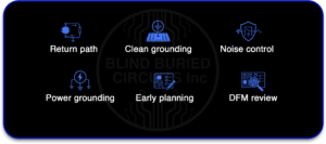
Table Of Contents
- Why Grounding Matters In Modern PCBs
- Why Grounding Is More Challenging In HDI PCB Design
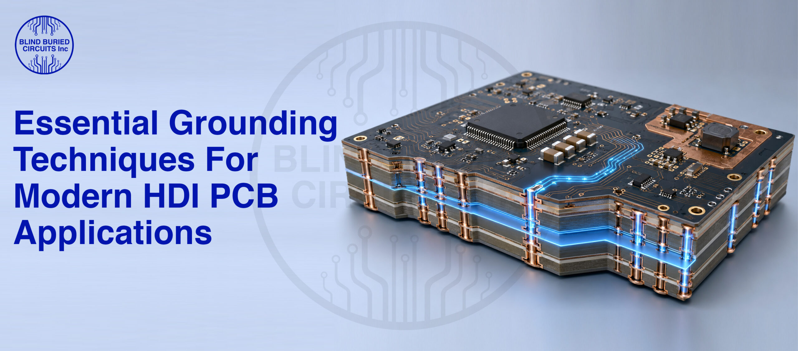
- Essential PCB Grounding Techniques For HDI Boards
- Return Current Paths In High-Speed HDI Boards
- Ground Plane Design Best Practices For Multilayer PCBs
- Power Integrity And Grounding In HDI PCB Design
- Grounding In Mixed-Signal And RF PCB Designs
- Grounding In High Power PCB Design
- How HDI PCB Manufacturing Affects Grounding Performance
- Signal And Power Grounding Checklist
- Common PCB Grounding Mistakes And How To Avoid Them
- FAQs
- Conclusion
Why Grounding Matters In Modern PCBs
Every circuit needs a return path. Current does not only move from the power source to a component. It also needs a path back. That return path is often ground.
This is why PCB grounding techniques matter. Good grounding gives current a short and clean path. Poor grounding makes current travel through long or broken paths. That can create noise, heat, voltage drops, EMI problems, and signal errors.
Ground provides the electrical reference and return-current path that directly affects signal integrity, EMI performance, and power integrity.
Modern boards are smaller than before. They also carry faster signals and more power. Phones, medical devices, sensors, control boards, RF modules, power converters, and wireless systems often use dense layouts. These designs need careful grounding from the start.
Grounding should not be treated as the last copper pour added after routing. It should be part of stack-up planning, component placement, power design, signal routing, and manufacturing review.
Why Grounding Is More Challenging In HDI PCB Design
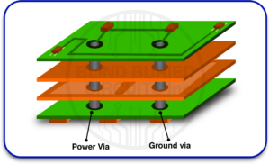
HDI means high-density interconnect. These boards use smaller traces, smaller vias, tighter spacing, and more compact routing. They may also use blind vias, buried vias, microvias, and fine-pitch components.
Good HDI PCB design helps fit more parts into less space. But it also gives designers less room for grounding mistakes.
In HDI boards, grounding is harder because parts sit closer together, signal paths are more crowded, and power and ground areas may be split into smaller regions. High-speed signals may switch very fast, while power sections may create heat and switching noise.
Microvias also need careful placement. When a signal changes layers, the return current needs a nearby ground path. If the design does not provide that path, current may spread through a larger loop and create noise.
A simple ground pour is not enough in HDI PCB design. The full stack-up must support clean return paths, stable reference planes, short decoupling loops, and practical manufacturing rules.
Essential PCB Grounding Techniques For HDI Boards
A solid ground plane is one of the most useful PCB grounding techniques. It gives signals a clean return path and helps reduce noise. In a multilayer board, try to keep at least one full layer as ground wherever possible.
Avoid cutting large gaps or slots in the ground plane. A split ground plane may look neat, but it can create return path problems. When a signal crosses a gap in the ground plane, the return current must go around the gap. This creates a larger loop, which can increase EMI.
Ground vias are also important. Use ground vias near signal vias, connectors, high-speed traces, RF sections, and shield areas. These vias help connect ground layers and give current a shorter path between layers.
Decoupling capacitors should be placed close to IC power pins. Fast chips need small bursts of current, and nearby capacitors help supply that current. Connect capacitors to ground with short traces and nearby vias. Long capacitor paths add inductance and reduce effectiveness.
Via stitching can also improve grounding. It connects ground copper across layers and helps create a stronger ground network. Use stitching near board edges, high-speed lines, connectors, RF areas, and shielded sections. But do not add vias without purpose. Too many vias can crowd the layout and affect manufacturability.
Return Current Paths In High-Speed HDI Boards
Every signal has a return current path. In high-speed boards, that return current usually flows close to the signal trace through the nearest reference plane. This is why signal routing and grounding must be planned together.
If a high-speed trace runs over a continuous ground plane, the return current has a direct path. If the trace crosses a split, slot, or broken plane, the return current must detour. That detour creates a larger loop area and can increase noise, crosstalk, and EMI.
Layer changes also need attention. When a signal moves from one layer to another through a via, the return current must also move to the correct reference plane. Ground vias placed near signal vias help provide that path.
This is especially important in HDI PCB design because dense routing often forces signals to change layers. Without nearby ground vias, the return path can become longer and less predictable.
Good return-current planning helps improve signal integrity, reduce EMI, and make board behavior more stable.
Ground Plane Design Best Practices For Multilayer PCBs
A good ground plane should be continuous, low impedance, and close to important signal layers. In multilayer PCB design, the stack-up should place ground layers near high-speed routing layers whenever possible.
Do not route fast signals over plane gaps. Do not split ground under clocks, RF traces, memory buses, or other sensitive signals. If a split plane is unavoidable, make sure critical signals do not cross the split.
Ground planes also help with shielding and heat spreading. A solid plane can reduce noise coupling between layers and provide a stable reference for controlled impedance routing.
For dense boards, it is better to plan ground layers early instead of trying to fix grounding after routing is complete. Once signals are already routed, it can be hard to repair broken return paths.
A well-planned ground plane supports better signal integrity, cleaner power delivery, lower EMI, and more predictable manufacturing results.
Power Integrity And Grounding In HDI PCB Design
Power integrity and grounding are closely connected. A board may have a solid power supply on paper, but poor ground design can still cause noise, voltage dips, and unstable circuit behavior.
Fast ICs need clean power and a low-impedance return path. Decoupling capacitors should be placed close to power pins, with short paths to both power and ground. The goal is to reduce loop inductance and keep power stable during fast switching.
Power and ground planes should be planned together. A strong plane pair can help provide distributed capacitance and improve high-frequency power delivery.
In HDI PCB design, space is limited, so capacitor placement, via location, and plane continuity become more important. Small layout mistakes can create noise problems that are hard to diagnose later.
Good power integrity planning helps reduce reset issues, data errors, EMI failures, and unstable performance during high-speed or high-load operation.
Grounding In Mixed-Signal And RF PCB Designs
Many modern boards include digital, analog, power, and RF sections. Each section behaves differently.
Digital circuits switch fast. Analog circuits read small signals. Power circuits carry larger current. RF circuits need stable impedance and low noise. Good grounding keeps these sections working together without allowing noise to spread everywhere.
For mixed-signal HDI PCB design, placement comes first. Keep noisy circuits away from sensitive analog and RF areas. Then use grounding to support that placement.
A common mistake is splitting grounds too much. In many cases, one strong ground plane with smart component placement works better than many broken ground regions. Too many splits can make return paths worse.
RF grounding needs special care. RF traces need controlled impedance, nearby ground reference, short return paths, and clean transitions. Ground vias are often used near RF lines, connectors, shields, and antenna feed areas to reduce unwanted radiation and improve stability.
The goal is not to isolate every section blindly. The goal is to control where current flows.
Grounding In High Power PCB Design
High power PCB design needs extra care because high current creates heat and voltage drop. If the ground path is too thin, too long, or poorly connected, the board can become unreliable.
Use wide copper areas for high-current ground paths. Keep power loops small. Separate noisy power sections from sensitive signal sections. Use enough vias for current sharing. Check copper thickness and thermal needs before layout release.
Avoid forcing high current through small traces or narrow vias. A motor driver, LED driver, charger, inverter, or power converter can create strong switching noise. Keep the switching loop short and place power parts close together.
Do not allow power ground noise to flow through sensitive analog, RF, or sensor ground areas. High-current grounding should be planned so large current returns do not disturb low-level signals.
Thermal planning also matters. Ground copper may help spread heat, but only when copper width, via count, copper weight, and layer connections are suitable for the load.
How HDI PCB Manufacturing Affects Grounding Performance
Grounding is not only a design topic. It also depends on HDI PCB manufacturing.
Small vias, microvias, buried vias, blind vias, tight spacing, copper thickness, and stack-up choices must match the manufacturer’s capability. A design may look good in software but become risky in production if the limits are pushed too far.
Ground vias must be manufacturable. Microvia size, depth, aspect ratio, and placement should be reviewed before final routing. If ground vias are too small, too dense, or poorly placed, they may increase fabrication risk.
Stack-up control is also important. Ground layers should be placed close to important signal layers. Copper weight should support current and thermal needs. Clearances should follow fabrication rules.
Before release, review these areas:
| Grounding Area | What To Review |
| Ground Plane | No unwanted gaps under key signals |
| Microvias | Proper size, depth, and placement |
| Stack-Up | Ground layers close to signal layers |
| Copper Weight | Enough for current and heat |
| Via Count | Enough for return and current sharing |
| Clearances | Safe for fabrication rules |
| Controlled Impedance | Ground reference supports target impedance |
Blind Buried Circuits supports advanced PCB structures where design rules, stack-up, and manufacturing limits must work together.
Signal And Power Grounding Checklist
Use this checklist before sending a board for review:
Is there a solid ground plane?
Are high-speed signals routed near a ground reference?
Are signal vias paired with nearby ground vias?
Are decoupling capacitors close to power pins?
Are high-current paths wide enough?
Are noisy power areas away from sensitive signals?
Are ground splits avoided where return current needs to flow?
Are RF traces referenced to stable ground?
Are analog and digital sections placed with noise control in mind?
Are microvias used within safe fabrication limits?
Is the stack-up confirmed before final routing?
Is copper weight suitable for current and heat?
Are ground vias used where layer transitions need return paths?
This simple check can prevent many common board issues before fabrication.
Common PCB Grounding Mistakes And How To Avoid Them
Grounding errors often happen because the board looks fine visually. But current does not care how the layout looks. It follows the path of least impedance.
Avoid using thin ground traces for high current. Avoid cutting ground planes under fast signals. Avoid placing decoupling capacitors too far from IC power pins. Avoid forgetting ground vias near signal vias.
Do not mix noisy power ground with sensitive analog or RF ground without planning. Do not change stack-up after routing without reviewing impedance, return paths, and grounding. Do not ignore thermal paths in high power PCB design.
Another common mistake is sending HDI files to production without checking fabrication limits. Microvias, copper spacing, layer registration, via count, and stack-up details can affect grounding performance.
Good grounding is not about adding more copper everywhere. It is about giving current the right path.
Conclusion
Good grounding starts before routing. It needs a clear stack-up, solid ground planes, short return paths, smart via use, controlled power planning, and careful manufacturing review. This is even more important in dense HDI boards.
When PCB grounding techniques are handled well, the board becomes quieter, more stable, and easier to test and manufacture. Good grounding can also improve signal integrity, power integrity, EMI performance, thermal behavior, and long-term reliability.
Blind Buried Circuits can support projects where HDI layout, controlled stack-up, high power PCB design, and reliable production need to work together.
Build the ground path first. A stable board starts with current that knows exactly where to return.
FAQs
What Are PCB Grounding Techniques?
PCB grounding techniques are layout methods that give current a clean return path. They include solid ground planes, short return paths, ground vias, via stitching, proper capacitor placement, and careful section planning.
Why Is Grounding Important In HDI PCB Design?
Grounding is important in HDI PCB design because parts are close together and signals often change layers. A poor return path can create noise, EMI, signal errors, and unstable board behavior.
Is A Solid Ground Plane Always Needed?
A solid ground plane is strongly recommended for most multilayer boards. It gives signals a low-impedance return path, improves signal integrity, and helps reduce EMI.
How Does Grounding Affect High Power PCB Design?
In high power PCB design, grounding affects current flow, heat, voltage drop, and reliability. Wide copper paths and enough vias help carry current without overstressing the board.
What Is The Role Of Ground Vias In HDI Boards?
Ground vias connect ground layers and help return current move between layers. They are especially important near signal vias, connectors, RF areas, and high-speed transitions.
Why Does HDI PCB Manufacturing Need Early Ground Planning?
HDI PCB manufacturing uses small features and tight spacing. Ground vias, microvias, stack-up, copper weight, and clearances must match real production limits before routing is finalized.


