
Objective
This blog explains PCB antenna design for hardware teams, buyers, founders, and students. It covers placement, layout, matching, materials, testing, and mistakes. Blind Buried Circuits works with complex PCB manufacturing, so this topic matters for connected products.
Key Takeaways
- A PCB antenna is part of the full board, not only one copper shape.
- Placement, clearance, stack-up, and nearby parts can change range.
- Good high-frequency PCB design starts early.
- A matching network helps the radio and antenna transfer power.
- Test the final product inside its real case.

Table Of Contents
- What A PCB Antenna Does In Wireless Devices
- Why PCB Antenna Design Matters
- Common Wireless PCB Antenna Types
- How Antenna Frequency Affects PCB Design
- High Frequency PCB Design Rules For Antenna Layout
- Controlled Impedance And RF Feed-Line Design
- Ground Plane Design Around PCB Antennas
- Signal Integrity PCB Checks For Wireless Boards
- PCB Stack-Up Considerations For Wireless Designs
- Common PCB Manufacturing Factors That Affect Antenna Performance
- Testing And Tuning PCB Antennas
- Common Mistakes To Avoid
- FAQs
- Conclusion
PCB antenna design is one of the most important parts of wireless product development. It affects range, signal stability, battery use, radio testing, and product reliability. A PCB antenna may look like a simple copper shape, but it works with the full board, stack-up, ground plane, case, battery, and nearby components.
This blog explains PCB antenna design for hardware teams, buyers, founders, and students. It covers antenna placement, layout, matching, frequency behavior, materials, testing, and common mistakes. Blind Buried Circuits works with complex PCB manufacturing, so this topic matters for connected products where wireless performance must be consistent from prototype to production.
What A PCB Antenna Does In Wireless Devices
An antenna turns an electrical signal into a radio signal. It also receives radio signals and sends them back into the circuit. This is how Bluetooth, Wi-Fi, GPS, IoT, and other wireless products connect without wires.
A wireless PCB antenna is made from copper on the board. It may be printed as a trace, shaped as an inverted-F antenna, meandered to save space, or designed as part of a larger RF structure. The antenna does not work alone. It depends on the ground plane, feed line, matching circuit, board material, and product enclosure.
A small change in antenna length, ground clearance, plastic housing, battery position, display placement, or nearby metal can shift antenna performance. That is why PCB design for wireless devices needs early planning. The antenna should not be placed after the rest of the board is finished.

Why PCB Antenna Design Matters
Strong wireless range does not come only from the radio chip. The PCB layout decides how much signal leaves the board and how much signal returns cleanly to the receiver.
Poor antenna design can cause short wireless range, weak signal through walls, higher battery use, failed radio testing, unstable links after the case is fitted, and different performance between prototype and production boards.
Good PCB antenna design helps the radio transfer energy efficiently into free space. It also helps reduce signal loss, reflection, detuning, noise coupling, and EMI problems. For wireless products, the board, antenna, case, and final assembly should be treated as one system.
Common Wireless PCB Antenna Types
Different wireless PCB antenna types are used based on product size, frequency, cost, and performance needs.
| Antenna Type | Best For | Main Point |
| Inverted-F Antenna | Bluetooth, Wi-Fi, IoT | Compact and common |
| Meandered Antenna | Small products | Saves space, but needs tuning |
| Chip Antenna | Tiny devices | Small, but needs good layout |
| External Antenna | Metal cases or long range | Easier to isolate from board noise |
| Monopole Trace Antenna | Simple wireless designs | Needs proper ground reference |
| Loop Antenna | Compact low-power devices | Useful where space is limited |
A wireless PCB antenna can keep costs low and work well in repeat production. Still, it must match the board size, housing, frequency, ground plane, and product use case.
Chip antennas are often selected when space is tight, but they are not automatically better. They usually need strict layout control, a proper ground plane, a matching network, and tuning in the final product. A PCB antenna can perform very well when the layout has enough space and the antenna area is protected.
How Antenna Frequency Affects PCB Design
Antenna frequency directly affects antenna size, trace length, ground plane behavior, material choice, and layout sensitivity. Lower-frequency antennas usually need more physical space. Higher-frequency antennas can be smaller, but they become more sensitive to layout changes, manufacturing variation, enclosure effects, and nearby components.
For example, many Bluetooth and Wi-Fi products operate around 2.4 GHz. At this frequency, the antenna, feed line, ground clearance, and matching network must be controlled carefully. Small layout changes can shift the antenna away from its target frequency.
At higher frequencies, PCB material properties also become more important. Dielectric constant, board thickness, copper roughness, solder mask, and fabrication tolerance can all affect impedance and signal loss. This is why high frequency PCB design should be reviewed before the layout is finalized.
The antenna must be designed for the real operating frequency, not just copied from another board. A design that works well on one product may fail on another if the board size, enclosure, battery, or ground plane is different.
High Frequency PCB Design Rules For Antenna Layout
High frequency PCB design is less forgiving than low-speed wiring. At radio frequencies, a trace becomes part of the circuit. The antenna, feed line, ground plane, and nearby copper all affect performance.
The antenna should be placed first when possible. Place the antenna at the board edge or corner when the reference design allows it. Keep it away from batteries, shields, screws, displays, motors, speakers, cables, and metal parts.
Do not bury the antenna inside a crowded layout. It needs open space to radiate. Many antennas also need a copper-free keep-out zone. This may mean no ground, no traces, no vias, and no components near the radiating section.
Do not guess the keep-out area. Use the antenna guide or reference design. A changed keep-out can shift the antenna frequency and reduce wireless range.
The RF path should also stay short and clean. Avoid sharp bends, unnecessary vias, long stubs, sudden width changes, and noisy routing near the antenna. In high frequency PCB design, small details can create large performance changes.
Controlled Impedance And RF Feed-Line Design
The RF feed line carries the signal from the radio chip or RF front end to the antenna. In many wireless designs, this feed line is designed for 50-ohm controlled impedance to reduce signal reflection and improve power transfer.
Controlled impedance depends on trace width, copper thickness, dielectric height, dielectric constant, ground reference, solder mask, and stack-up. If these details change during manufacturing, the real impedance can shift.
RF feed lines should be short, direct, and referenced to a stable ground plane. Designers often use microstrip or coplanar waveguide structures, depending on the board stack-up and antenna requirements. The correct structure should be calculated and confirmed with the PCB manufacturer.
A matching network is also important. It usually uses small capacitors and inductors between the RF output and the antenna. The matching network helps the radio and antenna work together. Leaving space for this network is important because those pads can save a board revision during tuning.
Ground Plane Design Around PCB Antennas
The ground plane plays a major role in PCB antenna design. In many wireless designs, the antenna needs a specific ground reference to radiate properly. Too little ground, broken ground, or copper placed in the wrong area can reduce antenna efficiency.
Some antennas need a clear copper-free keep-out area under and around the radiating section. Other antenna types depend on a specific ground plane size and shape. This is why the antenna layout guide should be followed closely.
Ground should be continuous near the RF feed line, but not placed where the antenna requires open clearance. Stitching vias may be used around RF traces or shielded sections, but they should not be added inside the antenna keep-out unless the antenna design calls for it.
Poor ground plane planning can cause detuning, weak range, EMI issues, unstable links, and inconsistent production results. Good ground planning helps the antenna behave more predictably across different units.
Signal Integrity PCB Checks For Wireless Boards
A clean antenna cannot fix a noisy board. That is why signal integrity PCB planning should happen early.
Before release, check that switching regulators are kept away from the RF path. Fast clocks should not be routed near the antenna. The radio chip should have clean power, stable grounding, and proper decoupling. Ground returns should remain continuous where high-speed signals change layers.
Noisy digital sections should be separated from RF sections. Motors, displays, DC-DC converters, high-current paths, and fast interfaces can inject noise into wireless circuits if placement and routing are poor.
Good signal integrity PCB work reduces noise in the radio path and helps units behave consistently. It also supports better wireless range, cleaner communication, lower packet loss, and more stable product performance.
PCB Stack-Up Considerations For Wireless Designs
PCB stack-up has a direct effect on antenna behavior, RF feed-line impedance, signal loss, and repeatability. For PCB design for wireless devices, the stack-up should be reviewed before routing begins.
Important stack-up details include board thickness, dielectric constant, dielectric loss, copper weight, solder mask thickness, layer count, reference plane location, and controlled impedance requirements.
FR-4 is common for many 2.4 GHz wireless products, but its properties can vary. For higher-frequency designs, more stable RF materials may be needed. The right material depends on frequency, cost, performance, product size, and manufacturing needs.
Blind Buried Circuits works with rigid, flex, rigid-flex, and HDI boards where stack-up control matters for wireless layouts. If the wireless board uses HDI routing, fine-pitch components, controlled impedance, or compact RF sections, the stack-up should be confirmed early with the PCB manufacturer.
Do not separate antenna design from manufacturing limits. A good layout can fail if the real board uses different material, thickness, copper weight, or spacing than expected.
Common PCB Manufacturing Factors That Affect Antenna Performance
PCB antenna performance can change during manufacturing if key fabrication details are not controlled. The antenna may be designed correctly in the layout file but still perform differently after production if material and process tolerances shift.
Board thickness is one important factor. If the dielectric height changes, the RF feed-line impedance can change. Dielectric constant variation can also shift antenna tuning and affect signal behavior.
Copper thickness and etching tolerance matter as well. A small change in RF trace width or antenna trace length can affect impedance and resonant frequency. Solder mask can also influence RF behavior, especially if it covers areas that were expected to remain exposed or controlled.
Surface finish, copper roughness, laminate type, panel variation, and fabrication tolerance can also affect high-frequency behavior. These changes may be small, but wireless designs can be sensitive to them.
For repeat production, the PCB manufacturer should understand which areas are RF-critical. Controlled impedance notes, material requirements, antenna keep-out areas, and fabrication tolerances should be clearly documented.
Testing And Tuning PCB Antennas
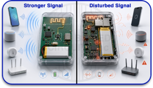
Testing should happen with the real product shape. Use the final case, battery, cable, display, mounting position, and nearby mechanical parts. A wireless PCB antenna should not be judged only from the PCB file because the finished device is the real antenna system.
Useful checks include return loss testing, antenna tuning, range testing, hand-held testing, enclosure testing, and sample comparison. A vector network analyzer is often used to check antenna matching and resonance.
If the antenna resonates too low, it may be too long. If it resonates too high, it may be too short. Matching parts can help tune performance without changing the whole board.
Testing should also compare multiple production samples. This helps confirm whether the design is stable across manufacturing variation. For wireless products, tuning only one prototype is not enough if the product will be built in volume.
Common Mistakes To Avoid
Many wireless problems come from simple layout and manufacturing choices.
Avoid placing copper under the antenna keep-out. Do not move the antenna from the reference design without review. Do not route clock lines, switching regulator traces, or high-speed digital signals near the antenna.
Do not forget the matching network. Do not place metal screws, shields, displays, batteries, or cables too close to the radiating edge. Do not change board thickness, material, copper weight, or enclosure design after antenna tuning without checking performance again.
Another common mistake is testing the antenna without the final enclosure. Plastic, metal, batteries, and even the user’s hand can affect antenna tuning. The final product must be tested as a complete wireless system.
Conclusion
Good PCB antenna design is not guesswork. It needs layout discipline, frequency awareness, material control, matching, testing, and common sense. The antenna should be planned early, placed carefully, and protected from noise, metal, and layout changes that can reduce performance.
For teams building wireless products, this approach can reduce delays and improve range. Blind Buried Circuits can support PCB manufacturing needs where layout quality, stack-up control, and reliable production matter.
Need a cleaner wireless board layout? Start with the antenna, protect the signal path, and build the PCB around reliable communication.
FAQs
1. What Is PCB Antenna Design?
PCB antenna design is the process of creating an antenna directly on the circuit board using copper traces. It requires proper antenna shape, ground clearance, matching network, feed line design, and tuning for the target wireless frequency.
2. Is A Wireless PCB Antenna Better Than A Chip Antenna?
Not always. A PCB antenna can be low-cost and efficient when there is enough board space and proper ground clearance. A chip antenna saves space but usually needs strict layout control, matching, and tuning.
3. Why Is High Frequency PCB Design Important For Antennas?
High frequency PCB design is important because small layout changes can affect impedance, radiation pattern, signal loss, and antenna tuning. The RF trace, ground plane, keep-out area, and matching network must be designed carefully.
4. How Does Signal Integrity PCB Planning Help Wireless Products?
Signal integrity PCB planning helps keep RF signals clean, stable, and low loss. It controls impedance, reduces reflections, limits noise coupling, improves grounding, and supports better wireless range and performance.
5. Can A PCB Antenna Work Inside A Plastic Case?
Yes. A PCB antenna can work inside a plastic case, but the enclosure can still affect tuning and performance. The antenna should be tested in the final product housing, with proper clearance from metal, batteries, displays, and other nearby parts.


