Request our manufacturing capability
Capabilities
Flex PCB Manufacturer
FLEX PCB – BLIND BURIED CIRCUITS
Blind Buried Circuits offers a wide range of Flexible printed circuit boards or bendable circuit board manufacturing and Flex PCB assembly in the USA, with various flex PCB material types and overlay options.
Flex PCBs are similar to Rigid PCBs, but when it comes to the comparison between flexible PCBs vs Rigid PCBs, Flex PCBs are getting popular due to their flex PCB design pattern and ease of fitting in any device where Rigid PCBs cannot used.
While many designers get worried while designing through the manufacturing capabilities of their chosen manufacturer, we encourage our customers to contact us when designing the flex circuit and considering flexible board material properties so our experienced engineering team can guide them over their design parameters to achieve maximum efficiency in electronic products.
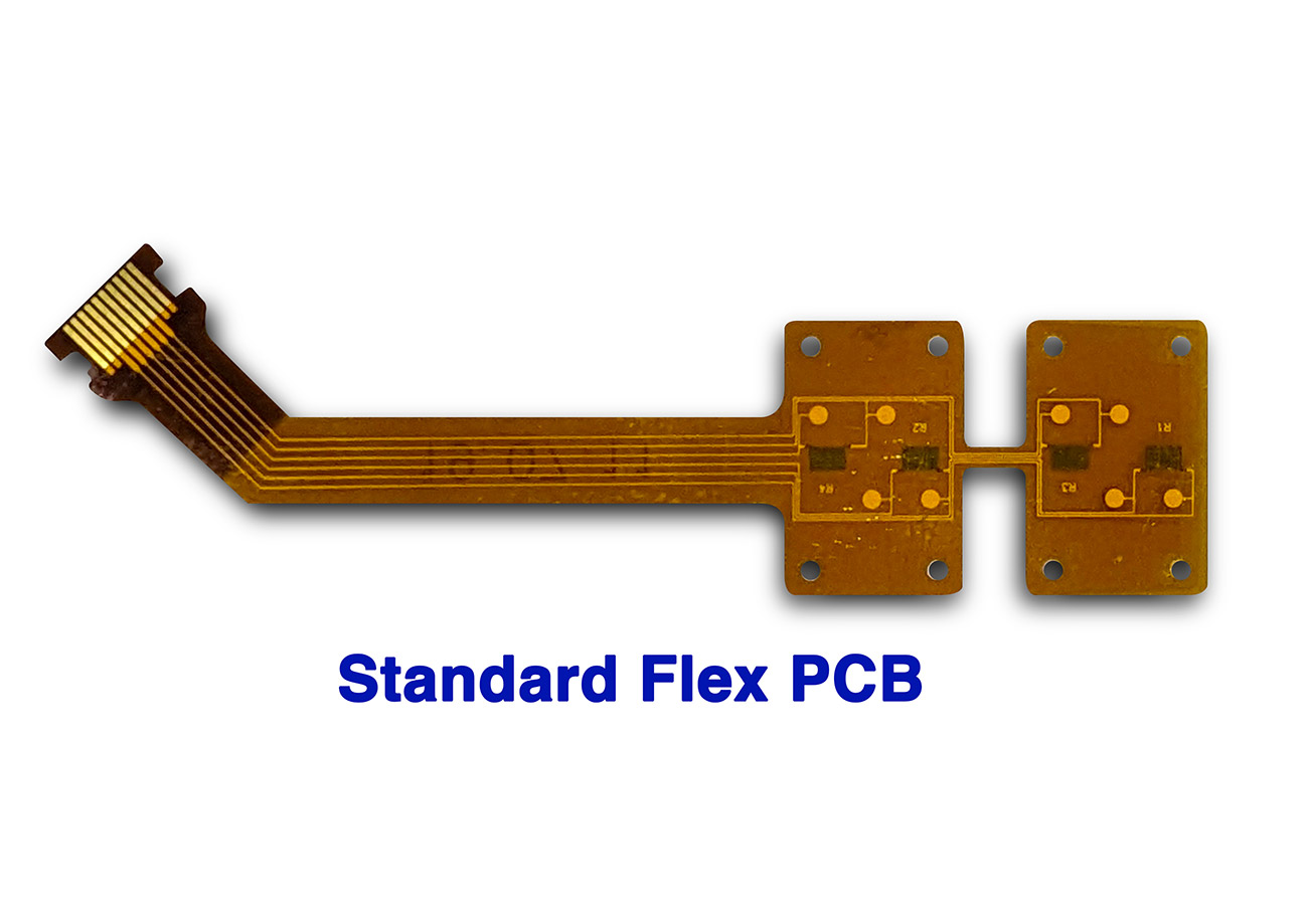
WHAT IS A FLEX PCB?
Flex PCBs are designed to fulfill product requirements where it needs flexible, bendable, and capable of fitting into tight spaces containing high temperatures. But to maintain the tight spaces, the flex PCB design requires flexible PCB material such as polyimide film substrates and PCB adhesive, flexible PCB stack up with conductive layers, tight tolerances, and special process treatments.
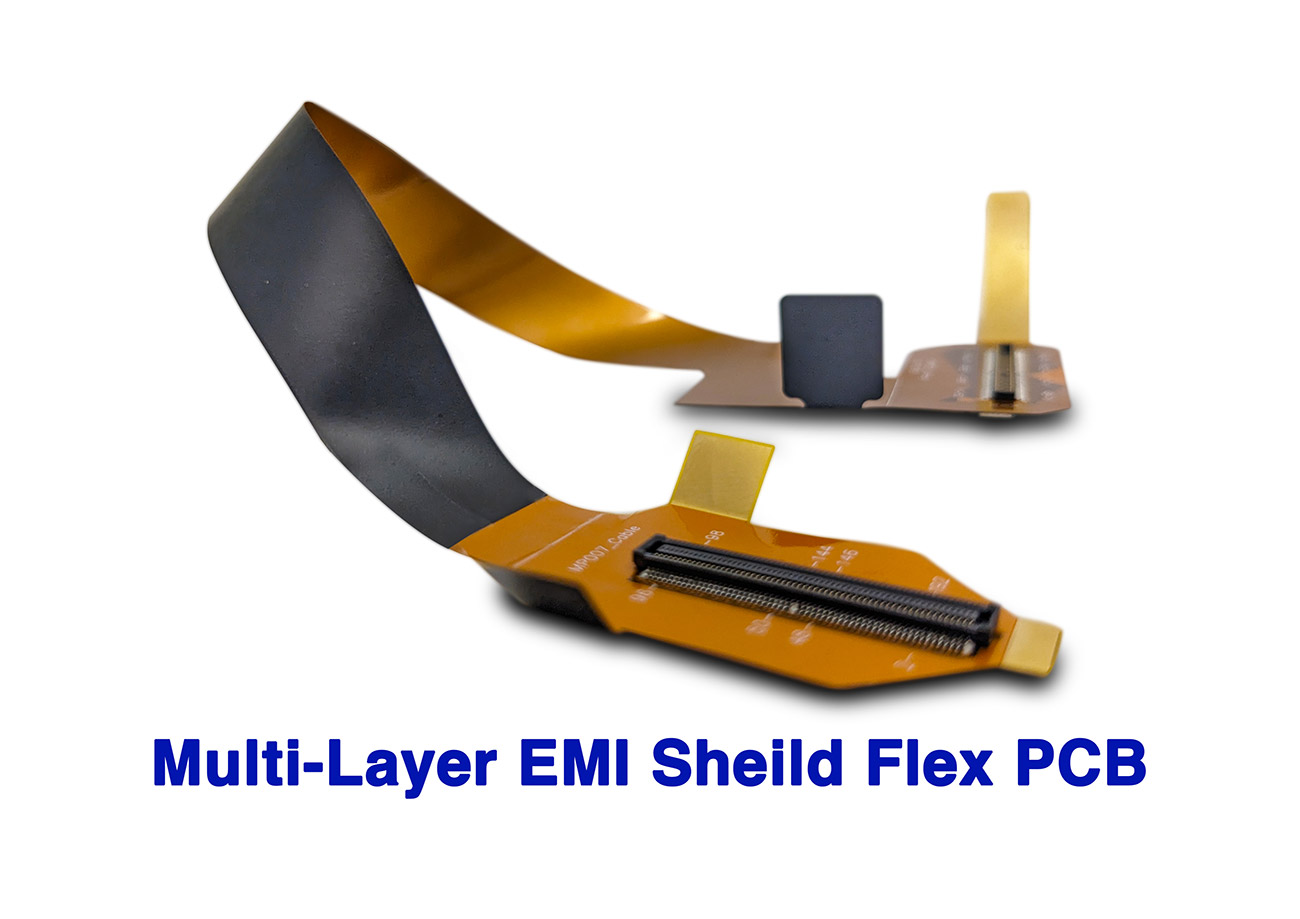
OUR MANUFACTURING CAPABILITIES
Blind Buried Circuits flexible PCB fabrication manufacturing capabilities include the following:
| Flexible PCB Material Selection | ||
|---|---|---|
| polyimide flexible PCB Subtract (Thickness) | 12 µm (0.0005”), 15 µm (0.005”), 25 µm (0.001”), 50 µm (0.002”), 75 µm (0.003”) | |
| Copper Clad (Thickness) | 9 µm (0.25 oz), 12 µm (0.33 oz), 17 µm (0.5 oz), 35 µm (1 oz), 70 µm (2 oz) | |
| Copper Foils (Rolled-Annealed) | Polyester, Polyimide, PIC (Photo Imageable Cover Coat), LPI (Liquid Photo Imageable) | |
| Stiffeners or flexible PCB insulation | Polyimide, Metal, FR-4, or customer supplied | |
| Thermo-Bond Adhesives | Phenolic Butyral, Acrylic, Modified Epoxy | |
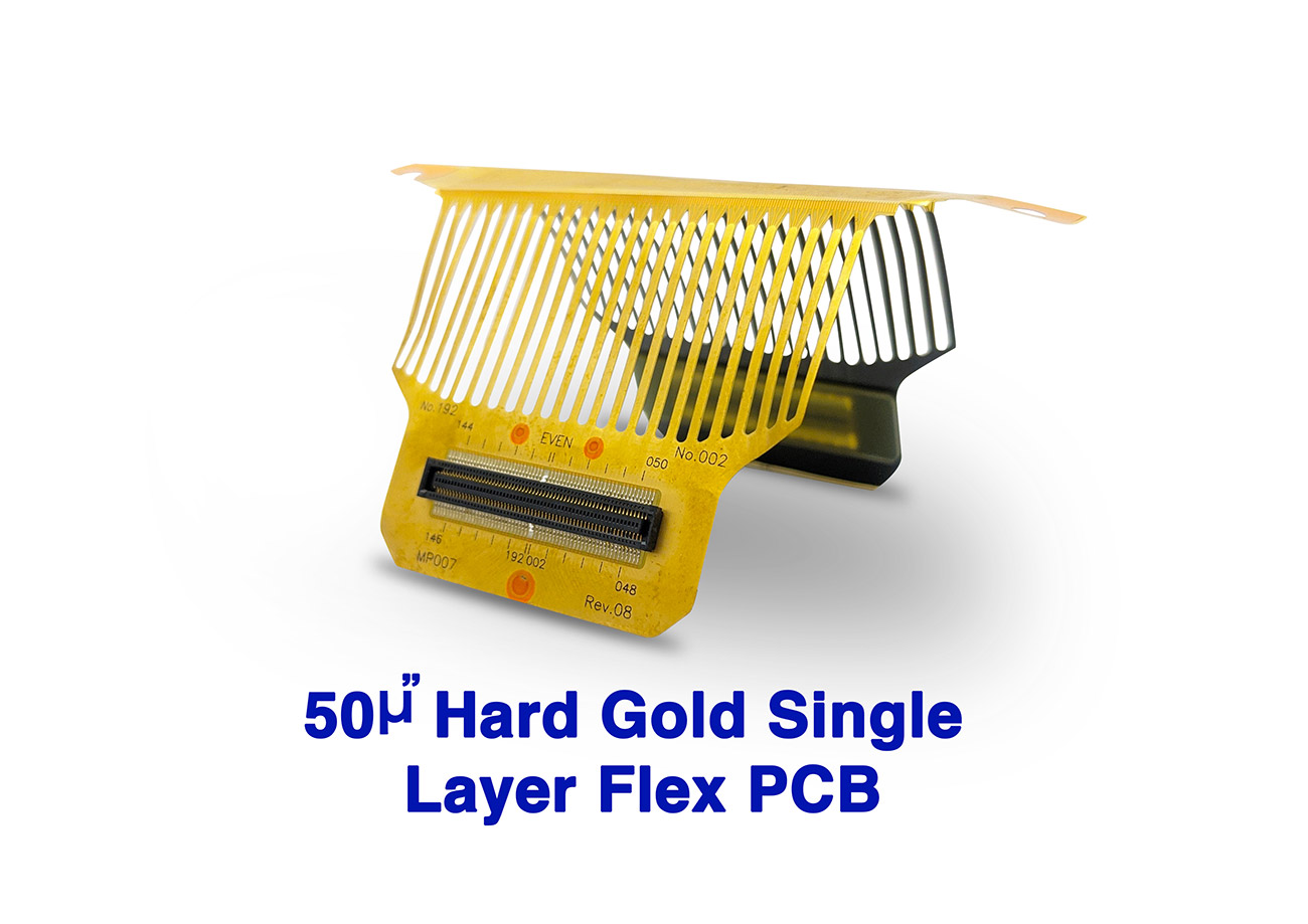
| Surface Finishes | Immersion Tin, Entek 106A, ENIG (Electroless Nickel Immersion Gold), Hard Gold, Electrolytic Soft Bondable Gold, Tin/Lead Plating, and Hot Air Solder Leveling | |
| Process Tolerances and Capabilities | ||
|---|---|---|
| Minimum Trace/Space | 0.0015”/0.002” for 0.33 oz copper 0.002”/0.0025” for 0.5 oz copper 0.003”/0.0035” for 1 oz copper | |
| Minimum Via Hole Dia (Before Plating) | 0.006” (NC Drill) 0.002” (UV Laser) | |
| Minimum Blind Via Dia (Before Plating) | 0.004” (UV Laser) | |
| Trace to Edge Distance | 0.010” for NC Routing 0.008” for Die Punch method 0.001” for UV Laser | |
| Trace to Edge Tolerance | 0.005” for NC Routing 0.003” for Die Punch method 0.001” for UV Laser | |
| Cover Layer Aperture Positional Tolerance | 0.005” for Cover Film 0.002” for LPI and PIC 0.001” for Laser Ablation | |
WHAT ARE THE BENEFITS OF FLEX PCBs?
All types of flex-printed circuit boards are used for various application benefits, whether making a wearable product or a phone; all PCBs play a significant role in product development. But when it comes to traditional Rigid PCBs, they are used for the very specific area where bendability doesn’t matter at all. But regarding wearable products like smartwatches, where a circuit needs to be bendable then Rigid PCBs don’t sustain there. That is when Flex boards help in completing the idea into the product. The following are the significant benefits of a flex circuit board:
- Reduced flexible PCB board thickness and weight: When it comes to ideal application, the designers always focus on low weight and thickness, attracting consumers to carry it easily. This is where Flexible PCBs play a vital role; the flexible PCB thickness is much thinner and lighter in weight than Rigid PCBs. The most common example of flex circuits is flexible PCB connectors.
- Improved flexibility: With products like flexible smartphones and wearable electronic items, the circuit needs to be in a specific shape to maintain the product’s form factor. Flex PCB board can be bent and flexed in any direction by considering and calculating the flex factor. Contact us if you have any questions regarding the flex factors for your PCB design or flexible PCB design guidelines.
We cater several Flexible Circuit Board markets
Consumer Electronics
We help companies that manufacture final products like smartphones, tablets, and wearable devices, or electronics products that consist of Flexible PCBs. These are widely used in consumer electronics due to their small form factor and flexibility.
Medical Devices
We have contributed to several top-notch medical products, which include diagnostic equipment, implantable devices, and monitoring systems. The flex PCB board is manufactured under controlled temperatures and with IPC Class 3 quality standards including visual inspection and printed circuit board testing to ensure there are no short circuits as per design
rules.
Aerospace and Defense
Our manufactured flexible PCBs are used in various lab test aerospace and defense system applications such as missiles, aircraft, and satellites.
Automotive Industry
With the revolution of electronic vehicles all over the globe, we have served various automotive applications such as safety systems, entertainment systems, and navigation systems.
Industrial Applications
Our flexible PCBs are implanted in industrial applications such as robotics, control systems, and sensors.
If you are looking for cost-effective, quick turn, high-quality flex or rigid-flex PCB manufacturing & assembly then do get in touch with our sales team at [email protected] if you have any questions or concerns regarding flexible PCB prototype and production.
frequently Asked Questions
- Avoid Plated Holes in the bend areas, “PTH Vias in bending regions can cause stress and failure.”
- Careful Placement of Vias near stiffeners, “Vias should not be placed just off the edge of stiffeners to prevent cracking.”
- Dynamic Flexing in applications with repeated bending, “Ensure Vias are not in flexing areas to avoid rapid cracking.”
- Teardrop Vias, “This helps to reduce stress on bendable area to Annular ring.”
- Add Tabs or Anchors to Vias, “This will help prevent peeling.”
- Use Curved Traces, “Avoid Trace with Sharp Corners as this reduces the chances of broken trace in bendable area.”
- Stagger Traces in Multi-layer Designs, “For Flex Circuits with 2 or more Layers, use stagger traces method on the top and bottom layers.”

