Request our manufacturing capability
Capabilities
Multilayer PCB MANUFACTURE
What is multilayer PCB?
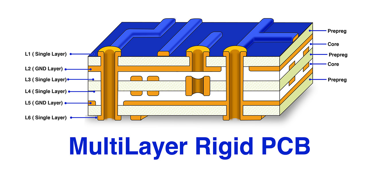
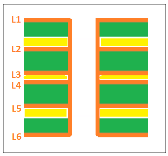
The Multilayer PCB's Structure:
| OUTER LAYER | ||
|---|---|---|
| DESCRIPTION | STANDARD | ADVANCED |
| Single / Double Sided | Minimum (7.874 Mils) & Max (314.96 Mils) | |
| Multilayer | Minimum (11.81 Mils) & Max (314.96 Mils) | |
| Bow & Twist | 3 to 7/1000 | |
Outer Layers:
The top and bottom conductive layers at which the majority of components are soldered are referred to as the outer layers.
Inner Layers:
There are additional layers of conductive copper that are known as the inner layers. Multilayer printed circuit boards (PCBs) can have several inner layers, including the top and bottom layers.
Prepreg:
The layers of insulating material that are used to separate the inner copper layers are referred to as prepreg. These are layers of fiberglass that have been partially cured and are used to apply the bonding agent between the layers.
Core:
Core works as insulating material, contains epoxy resin fiber glass, there are various types of RF & High speed dielectric substrate which also helps to prevent transmission signals in circuits with reference copper layers.
Vias:
- Through-Hole Vias: Vias that passes through all layers of PCB from top to bottom and giving connection to all layers
- Buried Vias: Vias that is buried in inner layers and not shown on outer layers. For example a via from 4th inner layer to 6th, 7th and 8th inner layer of PCB.
- Blind Vias: Vias that connect one of the outer layer to any internal layer.
- Copper Coin Via’s: Vias filled with copper solid coin are those meant to increase electrical conductivity and thermal performance by means of copper. these are usually applied into technologies which required high power and high speed circuits.
- Epoxy filled Vias: Epoxy filled Via’s are also known as non-conductive filled Via’s. This technology is applied to insulate heat and to reduce risk of solder paste wick on SMD pads where Via’s need to be placed.
Stackup of Multilayer PCBs:
When the structure of a multilayer PCB’s are taken into consideration, the arrangement of layers are decided according to design requirements including, ground, power planes and signal layers. Placement of layer are done with careful calculations with regard to signal integrity.
There are following consideration when one is planning layer stackup:
Applications of Multilayer PCBs:
- Telecommunications
- Automotive
- Consumer Electronics
- Medical Devices
- Industrial Automation
- Aerospace and Defence
- Computing and Data Centers
Our multilayer PCBs capabilities are designed to achieve the demands of todays and upcoming high density interconnect and complex circuit designs while maintaining a compact form factor. We aim to serve telecommunications, automotive, consumer electronics, medical devices, industrial automation, aerospace, defense, or computing & networking.
Our IPC A 600 & IPC A 610 engineering team ensures that every production must meet end user requirement including avoiding crosstalk with controlled impedance traces and with advance capabilities layer stacks from 1L to 60L layers, and critical features like copper coin via’s for enhanced electrical conductivity and thermal performance.

