Request our manufacturing capability
Capabilities
RIGID PCB Manufacturer
RIGID PCB BOARD
Rigid PCBs are the most conventional form of board in the PCB (Printed Circuit Board) world. They remain enormously popular today and are used in the majority of the electronics products industry.
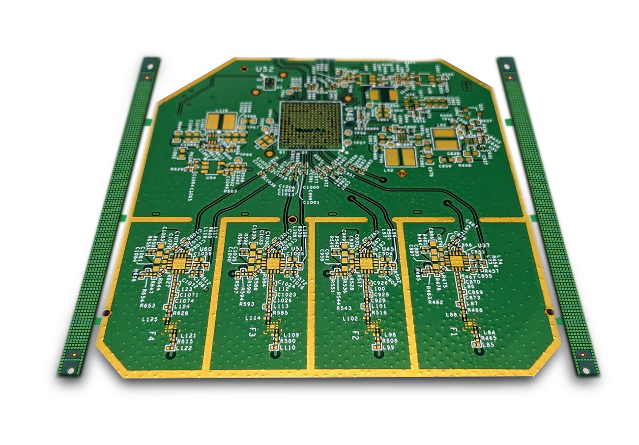
Blind Buried Circuit PCB Manufacturer Rigid PCB Capacity:
Rigid PCBs are manufactured in a solid state and inflexible in their structure; therefore, they cannot be flexed or bent. It comprises many unique layers, such as an electro-deposited copper foil, substrate/dielectric material consisting of Epoxy, Resin & Glass Fiber (Prepreg), stacked together through thermal pressure lamination.
Circuit design and manufacturing of Rigid PCBs are based on stack constructions which can be single-sided, double-sided & multilayered. Rigid PCBs can take any of these depending on the requirements. However, once manufactured, they cannot be delaminated/changed or modified.
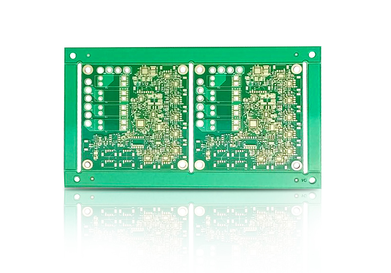
Benefits of Rigid PCB
Rigid PCBs are specifically famous in electronic industries including (medical, consumer electronics, industrial & communication) and products where elements must remain fixed, as they can survive with both high levels of stress and thermal heat during their performance and maintain product quality.
There are various high-temperature substrates in rigid pcb manufacturing such as low glass flow prepreg/dielectric material for RF stacks and all exotic materials including 370HR, FR408 HR, Rogers, Nelco, Panasonic Megtron.
At Blind Buried Circuits, we provide our customers with high-quality Rigid PCB by understanding board design and the manufacturing process needed as per their requirements including low glass flow prepreg/dielectric material for RF stack-ups and high-speed Circuits.
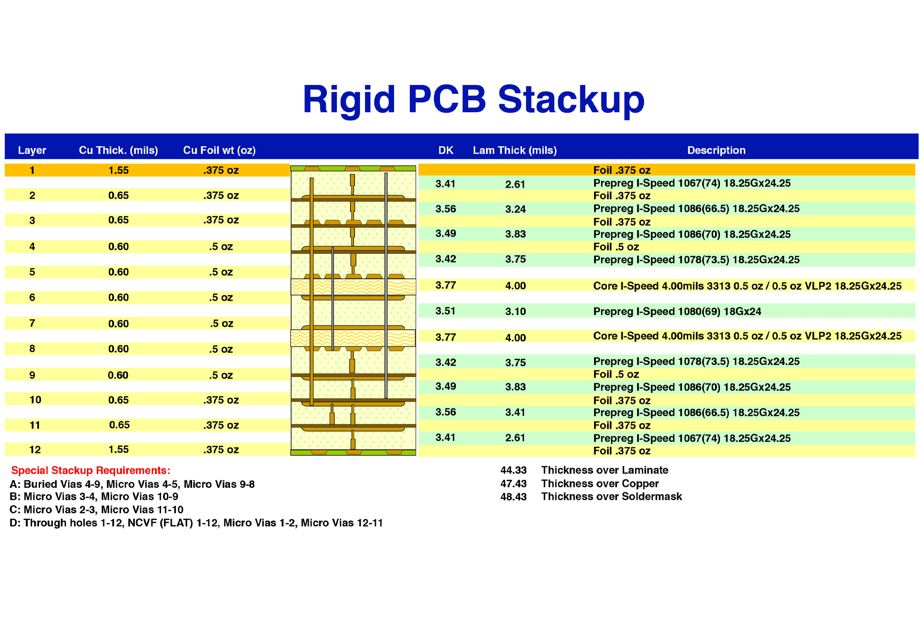
Blind Buried Circuits Manufacturing Capabilities for Rigid PCB Board
| LAMINATION | ||
|---|---|---|
| DESCRIPTION | STANDARD | ADVANCED |
| Layer Count | 1L to 50L | 60L |
| Layer to Layer Registration | +/-4mils | +/-2mils |
| Layer to Layer Prepreg Tolerance | +/-10mils | |
Blind Buried Circuit Advance Capabilities for Rigid PCB Boards
The other capabilities when it comes to rigid PCB boards (Printed Circuit Board) are as follows;
- UL and ISO 14001, ISO 13485 & ISO 9001 Certified
- RoHS (Restriction of Hazardous Substances) Compliant
- 2/2 mil Trace width and Spacing
- Blind Vias / Micro VIA’s (stacked & staggered)
- Buried Vias
- Minimum Laser Drill Size 3 mil
- Controlled Impedance with tolerance (-/+10%)
Blind Buried Circuit Advance Capabilities for Rigid PCB Boards
Rigid PCBs (Printed Circuit Boards) are applicable in various day-to-day devices that we depend on for communication such as:
- Mobile Phones
- GPS Equipment
- AC/DC Power Convertors
- Transmission Sensors
- Computers
- Tablets
- Laptops
Additionally, they are applied in essential medical equipment they are generally used in large, non-portable devices such as:
- CT (Computed Tomography) Scan
- X-Rays
- MRI (Magnetic Resonance Imaging) Systems
- EMG (Electromyography) Machines
- Heart Monitors
PCBs (Printed Circuit Boards) can survive in high temperatures with the help of exotic material & copper substrates, which means that they are also excellent for the aerospace industry, where they are applied in a range of important equipment.
- Power Convertors
- Temperature Sensors
- Control Tower Instrumentation
- Aeroplane Cockpit in Instrumentation
Don’t hesitate to reach out to us if you have any problems, questions or concerns regarding the Rigid PCB prototype and production. You can get more information from our sales team at sales@blindburiedcircuits.com.
Our Capabilities
CAPABILITIES OF BLIND BURIED CIRCUITS
- PCB layout design (Rigid 2-20 Layers & Flex circuits 2-6 Layers)
- Turnkey PCBA (Fabrication, parts procurement & Assembly Labor)
- High-Frequency PCB (Printed Circuit Board),
- LED PCBs,
- Thick-Copper Clad PCBs,
- HDI (High-Density Interconnect) PCB,
- Full Turnkey PCB (Printed Circuit Board),
- Rigid PCB,
- Flex PCB,
- Rigid-Flex PCB,
- Metal core PCBs,
- Critical finepitch parts soldering/assembly,
- minimum 0.4mm BGA assembly,
- 01005,0201 and other discrete parts packages
- QFN, QFP, LGA, SOIC’s & Leaded assemblies & No lead Assemblies.
Difference Between a Rigid PCB And a Flex PCB:
| RIGID PCB | FLEX PCB |
|---|---|
| The rigid PCBs are inflexible in structure. | The flex PCBs can be bent or otherwise shaped because they are flexible. |
| It is made up of a Rigid core with minimum thickness of 0.031” (+/-4mil), silk screen, and a solder mask. | It is made up of a flexible polymide core of minimum 1 mil, and stiffeners (FR4 and or Stainless Steel) are used for rigidity towards component placement locations, Silkscreen, PSA (Pressure Sensitive Adhesives), and Cover-lay (similar to Solder Mask) |
| It is used in desktop computers and televisions. | It is used in wearable technology and smartphones. |
Why Would You Choose Blind Buried Circuits
- Always Available For You: Blind Buried Circuits has been committed to providing 24/7 customer service to all our customers in the USA and Canada with cost effective manufacturing.
- Our Experienced Team: We have a highly experienced and knowledgeable team of IPC-certified engineers who run DFM & DFA before manufacturing to avoid any risk of failures in production.
- Our Fast Delivery: You will get an advantage from the fastest lead times all over the USA and Canada. To ensure we meet your turnaround deadlines. This is why most of our customers are dependable to us and get weekly/daily updates on their projects.
How to get a quote for Rigid PCB Board
frequently asked Questions
We recommend balancing the dielectric thickness, which could reduce the warpage or twisting to within 7 parts per thousand or less.
For example: If a PCB width is 500mm long then the standard bow and twist allowance should be under 3.5mm.

