Request our manufacturing capability
CAPABILITIES
PCB thick copper pcb manufacturing & assembly
WHAT ARE THICK COPPER PCB:
Thick Copper PCB are technically heavy copper PCBs manufactured at higher copper weight to accommodate high current printed circuit board designs. Whereas the standard PCBs are made at 1 to 2 Oz copper weight, mechanical stability, and easy heat flow are essential for high-power industrial electronics to operate efficient circuitry. At Blind Buried Circuits, we provide high-quality Thick-Copper PCBs up to 12 Oz thick. Not only our lead times are quick, but we ensure efficient manufacturing and quality.
Please fill out our quote form and select the required Hi-TG material for a quick offline quote

Blind Buried Circuits Thick-Copper PCBs Manufacturing Capabilities:
With the right expertise, dedicated people, and state-of-the-art infrastructure, Blind Buried Circuits can accommodate all types of PCB manufacturing, including thick or heavy copper PCB manufacturing. We ensure that our experts engage with you to understand all your manufacturing requirements and help to achieve your goals by keeping it cost-effective and the best in quality. Our capabilities include the following:
- Layers Count: Min 1 layer | Max 50 layers
- Materials: Arlon, Taconic, Nelco, Isola, and Rogers
- Board Thickness: Min 0.011″ to 0.0039″ | Max 0.393″
- Copper Thickness: Upto 12 Oz
- Solder Mask Colors: Green, Blue, White, Red, Yellow, Black
- Silkscreen Colors: White, Yellow, Black
- Surface Finishes: Leaded HASL, Lead-free HASL, ENIG, Immersion silver, Immersion Tin, OSP, ENEPIG, and bare copper
- Manufacturing lead time: 5 Days to 2-3 weeks
- MOQ = No minimum order quantity requirement
- We provide express deliveries in the United States and Canada, including Wisconsin, Massachusetts, New York, Ohio, Washington DC, and Texas.
The Manufacturing Process Behind Thick Copper PCBs
Are you seeking high-quality and dependable printed circuit board fabrication in
At Blind Buried Circuits, the manufacturing process of thick copper PCBs is optimized to ensure quality and precision. From selecting the right copper foil to managing the production process, our team follows a stringent set of procedures. This allows us to reduce production lead time while maintaining the highest standards of quality. With advanced technology, we ensure that trace width and copper layers are meticulously maintained to provide superior results.
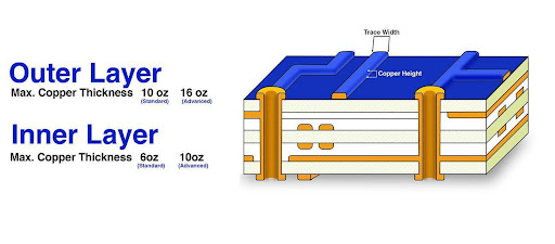
Copper Thickness
OUTER LAYER | ||
DESCRIPTION | STANDARD | ADVANCED |
Min. Trace/Space | 2.5mils / 2.5mils | 2mils / 2mils |
Max. Copper thickness | 10 oz | 16 oz |
Min. Copper Thickness | 0.6 oz | |
INNER LAYER | ||
DESCRIPTION | STANDARD | ADVANCED |
Min. Trace/Space | 2mils / 2mils | 1.5mils/1.5mils |
Min. Copper Thickness | 1/3oz | 1/7 oz |
Max. Copper thickness | 6oz | 10oz |
Defining Copper Thickness and Its Role in High-Performance PCBs
Copper defined in terms of copper thickness plays a significant role in the functionality and durability of high-power electronics. By using thicker copper, our PCBs offer improved heat dissipation, enhanced electrical conductivity, and higher reliability for industries such as automotive and defense. Blind Buried Circuits ensures that the copper foil used in our manufacturing process meets stringent quality standards for superior performance.
Advantages of using Thick-Copper PCBs for your applications:
Using Thick-Copper PCBs for applications with high power or current requirements has multiple advantages. Following are the advantages that you can find by manufacturing your Thick-Copper PCBs at Blind Buried Circuits:
- Can handle disclosure to high levels of current.
- Thermally resistive
- High tolerance rate
- Better conductivity and interconnection strength
- Fewer chances of failure rate due to better connections
- Reduced production cost
Enhancing Power Capabilities with Thick Copper PCBs
The ability to enhance power in high-current applications is a key advantage of using thick copper PCBs. At Blind Buried Circuits, our thick copper PCBs are designed to support power-intensive systems such as DC-DC converters and electric transformers. The use of copper layers and high-quality raw materials ensures that our boards deliver efficient performance while maintaining mechanical stability under high current loads.
Applications of Thick-Copper Printed Circuit Boards:
With great uses, various applications use thick-copper PCBs; these industries include power, nuclear, automotive industry, military, and defense. The applications which use Thick-Copper PCBs include:
- Power and amplifier modules
- DC-DC converters
- Electric transformers
- High-temperature products
- Automotive electrical junction boxes
- High-power distribution circuits
- Arms control systems
- Radar system
- Monitoring systems
- Electric Battery chargers
- Power Electronic Appliances
Optimizing Copper Traces for High-Current Applications
The design and layout of copper traces are crucial for the performance of thick copper PCBs in high-current applications. Our engineers at Blind Buried Circuits focus on optimizing the trace width to handle large currents while minimizing resistance and heat buildup. This design strategy ensures the longevity and reliability of power modules, electric transformers, and automotive electrical junction boxes.
Considering the quality, we have served the electronic industry with a highly dedicated team and exceptional manufacturing capabilities to complete the production within the quoted lead time. To know more about our capabilities or want a quick quote from our sales team, please submit your quote request or email us at sales@blindburiedcircuits.com to get a quote from Blind Buried Circuits. We are available 24/7 to help our customers in the United States, and Canada make their products a reality.


