Printed Circuit Boards (PCBs) are at the heart of modern electronics, enabling functionality across industries like telecommunications, medical devices, automotive systems, and more. As technology advances, the demand for compact and high-performance PCBs has skyrocketed. This is where High-Density Interconnect (HDI) routing plays a pivotal role. In this blog, we’ll explore the essential HDI routing techniques required for high-performance PCBs while focusing on the importance of custom PCB production and efficient PCB routing.
What is HDI Technology?
HDI technology is about designing PCBs with a higher density of interconnections, finer lines, smaller vias, and more compact designs. This enables manufacturers to pack more functionality into smaller spaces, which is ideal for applications that require miniaturization and performance.
At its core, HDI design includes micro vias, blind and buried vias, and thin traces to interconnect components without sacrificing performance. These features make HDI PCBs an integral part of advanced electronics, especially in devices like smartphones, tablets, and medical instruments.
Advantages of HDI Routing for PCB Design
Applying HDI routing techniques in custom PCB manufacturing offers several benefits, such as:
- Compact Design:
HDI PCBs allow manufacturers to miniaturize their electronic devices by integrating as few but more complex functions into tiny spaces. This is significant for portable devices and space-constrained applications.
- Performance enhancement:
The signal path reduction feature in HDI PCBs minimizes signal loss and improves the transmission speed, which is important for high-frequency applications.
- Enhanced Reliability:
HDI design uses blind and buried vias to reduce the stress level on interconnections, hence improving durability and reliability.
- Cost Effectiveness for Long-Term:
Higher HDI PCBs might have relatively high manufacturing costs, and with fewer layers and minimizing the usage of material, the benefits in the long run might come at a considerable cost advantage.
Key HDI Routing Techniques
For high-performance PCBs, effective key techniques in HDI must be adopted. Let’s discover some of the core best practices:
- Use of Microvia:
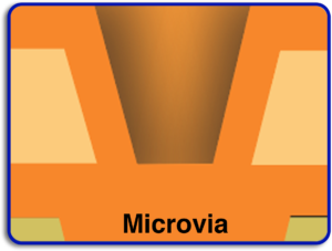
Microvias are a characteristic feature of HDI PCBs. They allow connections between layers to be made by using very small laser-drilled holes. These vias decrease parasitic inductance and improve signal integrity with a high-speed design requirement.
Best Practice: Implement stacked microvias to use multi-layer interconnections or staggering microvias to create more space and reliability improvement.
- Blind and Buried Vias:
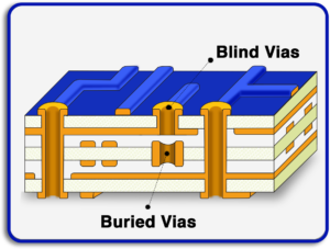
Blind vias connect outer layers to inner layers, while buried vias connect internal layers without reaching the surface. These features allow more routing space and reduce board thickness.
Best Practice: Strategically place blind and buried vias to optimize space for signal routing and power distribution.
- Fine Trace and Space Widths:
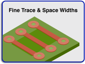
HDI PCBs require ultra-thin traces and minimal spacing to accommodate high component densities. This ensures efficient routing without interference.
Best Practice: Ensure trace widths are uniform and control impedance techniques for high-speed signals.
- Stack-Up Design:
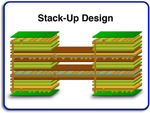
The optimized stack-up reduces crosstalk and EMI but ensures signal integrity.
Best Practice: Use good dielectric materials and maintain spacing between layers for thermal and electrical performance.
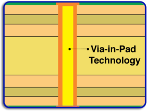
- Via-in-Pad Technology:
This technique uses vias directly placed underneath the pads of components, saving space and allowing for better thermal dissipation.
Best Practice: Fill and plate via holes to prevent solder wicking and ensure smooth assembly.
Challenges in HDI PCB Routing:
High-Density Interconnect (HDI) PCBs offer compact designs and enhanced functionality but present several challenges in routing and manufacturing.
- Manufacturing Complexity:
Creating microvias and managing fine traces demand advanced equipment and precise techniques. Microvias require laser drilling with minimal tolerance for errors, while fine trace spacing necessitates high-resolution imaging and etching. Misalignment in multilayer stacks can disrupt functionality, making exact layer registration critical.
- Higher Initial Costs:
HDI PCBs involve specialized equipment, skilled expertise, and iterative prototyping, increasing upfront expenses. Although initial costs are high, the benefits in performance and size often justify the investment.
- Thermal Management:
Dense layouts limit space for heat dissipation, leading to potential overheating. Effective thermal management involves using materials with high thermal conductivity, thermal vias, and copper planes to manage heat without adding complexity.
- Signal Integrity Issues:
Compact designs can lead to electromagnetic interference (EMI), crosstalk, and signal loss. Maintaining controlled impedance, minimizing reflections, and using advanced simulation tools are essential to address signal integrity concerns.
To overcome these challenges, collaboration with experienced manufacturers, adherence to design-for-manufacturability (DFM) principles, and robust prototyping processes are crucial for successful HDI PCB implementation.
Comparing HDI PCBs to Traditional PCBs
|
Feature |
HDI PCBs |
Traditional PCBs |
| Layer Count | Up to 50 layers | Typically up to 16 layers |
| Via Types | Microvias, Blind, Buried | Through-hole |
| Trace Width/Spacing | As small as 2 mils | 6 mils or larger |
| Application | High-speed, compact designs | General-purpose electronics |
| Manufacturing Cost | Higher initial cost | Lower initial cost |
| Signal Integrity | Enhanced | Standard |
In the current electronics world, it is crucial to master HDI routing techniques for a high-performance PCB. From microvias to via-in-pad technology, these methods support compact, efficient, and reliable designs. At Blind Buried Circuits, our strength in custom PCB production and advanced PCB routing guarantees great results for your project. Contact us now, and let’s bring those innovative designs to life!

