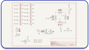
A schematic diagram is an essential part of electronics because it shows how different parts of a circuit are connected. Whether you are a custom PCB producer or a simple user trying to understand an electrical schematic, a circuit schematic is essential for knowing the current direction and the connection of different parts.
Schematic Symbols Standardization
Schematic Symbols are standardized all over the world to create uniformity for different industries and projects. The most applied ones include:
- IEC 60617: This standard is published by the International Electrotechnical Commission and includes over 1750 schematic symbols.
- ANSI Y32: Originally provided by the American National Standards Institute, this standard was used in aircraft applications and was later adapted for general use.
When these standards are used, it ensures that the engineers and technicians will comprehend the schematics regardless of where they were drawn.
Common Schematic Symbols
Every component of a schematic has a corresponding symbol that represents its function. A shorthand for resistors, capacitors, diodes, transistors, etc., is captured by these symbols. Let’s look at some of the most common symbols used:
| Component | Symbol | Reference Designator |
| Battery | BT | Provides power |
| Resistor | R | Limits current |
| Capacitor | C | Stores energy |
| LED | LED | Emits light |
Knowing how each of these symbols is used is essential in reading schematics.
Values and Attributes in a Circuit Schematic
Each component in the circuit schematic has some specific values and attributes to go with its purpose. For example:
Resistors: Ohms (Ω) with attributes like tolerance and wattage.
- Capacitors: Farads (F), plus a voltage rating.
- Inductors: Henries (H) and a current rating.
- Batteries: Voltage and capacity.
Reference designators, like R1, tell us what the schematic component is. In this case, R1 is a resistor.
Understanding Units in Schematic Diagrams
In electronics, values can be extremely small to very large. To normalize this, engineers use SI (International System of Units), which utilizes these prefixes:
| Prefix | Symbol | Value |
| Kilo | k | 1,000 (10^3) |
| Mega | M | 1,000,000 (10^6) |
| Micro | μ | 0.000001 (10^-6) |
| Nano | n | 0.000000001 (10^-9) |
Schematics become more interpretable and less cluttered with the use of these prefixes.
Schematic Diagram vs. Wiring Diagram
Wiring and schematic diagrams might seem similar, but they have different functionalities:
- Schematic Diagram: Displays connections among the components without consideration of their actual locations.
- Wiring Diagrams: It depicts the arrangement of wires and their components and accurately describe how the connection is made in reality.
Even though schematic diagrams effectively show how the circuit works, wiring diagrams are instrumental in assembly and fault finding.
How to interpret a Schematic Diagram of a PCB
To read a PCB schematic for the very first time can look like a daunting task, but it can be made easier by taking it small chunk by small chunk:
- Identify the Power Source: Look for the battery or power supply symbol to determine where the circuit starts.
- Follow the Nets: Connectors of the components are joined with nets (lines) to show the direction of electricity.
- Look for Junctions and Nodes: Nodes represent the joining of several connections in a single place.
- Check for Net Names: In some circuits, labels are used instead of direct connections to prevent messy connections.
- Understand Operating Conditions: Usually, components have their voltage, current and power rating printed on them.
A circuit or schematic can be built up and examined by following these steps.
How to Produce a Schematic Diagram
Making a precise schematic is the first and one of the most important processes in custom PCB fabrication. Here is how you can do it.
- Choose a PCB Design Tool: Some software, such as Altium, Eagle, and KiCad, can generate schematic diagrams.
- Define the Circuit Function: Before starting, it’s important to know the intention behind this circuit. This knowledge is crucial to aid in the proper arrangement of the components.
- Place Components with Care: Group the components according to their logical connections.
- Connect Components with the Use of Nets: Indicate electrical connections using lines.
- Assign Values and Attributes: Add component values and reference designators in a neat manner.
- Check for Mistakes: Look for connections and values that were mistakenly left out.
- Carrying out these processes guarantees a schematic that is clean and devoid of errors.
Guidelines for Conducting Schematic Diagrams
The following steps will help you come up with a good schematic, do the following:
Arrange Components: Place components that are related next to each other.
- Maintain Even Spacing: Maintain consistent spacing between lines and components.
- Do Not Cross Lines: If possible, cross labels rather than lines.
- Name Significant Nets: Label power and ground connections appropriately.
- Add a Title Block: Include details such as project name, revision number, and date.
Proper schematic design is one of the most important aspects of the success of the PCB manufacturing process.
Naming the Schematic Nets
Rather than drawing every single connection, engineers create named nets to make the schematic less cluttered and easier to understand. For instance, the VCC net in a circuit is understood to connect everywhere else with the VCC label. This makes diagrams easier to read and understand.
The Variance Between a Schematic and a PCB Layout
A schematic diagram displays the logical connections between components, while a PCB layout shows the actual arrangement of the components. Both are needed in the production of a PCB so that the particular design works and can be easily made.
While every time conceptual schematics are given with PCB layout, the following elements are looked at as well:
- Placement of components
- Integrity of signals
- Management of heat
Familiarization with both parts of the layout makes a project efficient.
Final Remarks
Schematic diagrams are crucial features in every electronics venture. They quickly capture how every electrical component is interlinked, making it easy to design, test, and build a circuit. From simple systems to custom PCBs, a working knowledge of electrical schematics is needed.
With the right knowledge of schematic symbols and values, circuit schematic design can become a mastered activity for anyone. Therefore, before tackling a particular project, always bear in mind that an appropriate schematic has to be drawn.
Need someone to help you design your PCB? Contact us now and find out how we make PCBs.


