The electronics industry is changing rapidly, with High-Density Interconnect (HDI) PCBs at the center of this transformation. This paradigm includes everything from smartphones and wearables to Internet of Things (IoT) devices.
Given the increasing need for compact, quicker, and more dependable devices, the manufacturing of HDI PCBs is becoming increasingly important. This blog will go through some of the best practices for PCB board makers in Manufacturing HDI PCBs, which will help them streamline their workflows, improve product quality, and achieve optimal accuracy.
What Is An HDI PCB?
Let’s first understand what HDI PCBs are before we delve deeper into the best practices. High-density interconnect PCBs are advanced PCBs that utilize a highly elevated compendium of components and increased connections.
In comparison with traditional PCBs, HDI boards employ micro vias, narrower traces, and smaller components to integrate a higher level of functionality within a small area. This enables manufacturers to produce devices that are smaller, faster, and incredibly reliable with no performance limitations.
Space constraints paired with high performance and reliability requirements for smartphones, tablets, laptops, medical devices, and automotive electronics make HDI PCBs increasingly desirable.
Best Practices in HDI PCB Manufacturing
HDI PCBs are strategically designed and manufactured to satisfy high-end requirements and thus need a great deal of precision. Below are some key practices every HDI PCB manufacturer should consider to increase output and performance:
-
Design Considerations
One of the most important steps to take when developing an HDI PCB is the design step. It is critical to note that the design of the PCB determines the ‘manufacturability,’ performance metrics, and profitability of the final product. Consider the following:
- Exact Alignment: Components and routing need to be exceptionally well aligned to avoid defects associated with poorly manufactured HDI PCBs, especially at high-density interconnects since they are closely packed.
- Choice of Material: The type of material to use for the PCB substrate is essential. The most frequently used materials in HDI PCBs are FR4, polyimide, and ceramics. The type of material used should provide sufficient strength for the application’s thermal, mechanical, and electrical conditions.
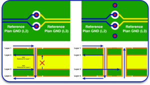
- Integrity of the Signal: Since the number of components packed inside the assembly is very high, signal loss makes this feature very sensitive. Adequate routing methodology and impedance control techniques should be applied to eliminate interference and signal loss.
-
Optimum Layout Design
A properly planned layout is essential for the precise manufacturing of the HDI PCB. Correct component arrangement and routing are crucial to the PCB’s performance. The placement of components is arranged so that signals are not disturbed, and functions are optimized. This reduces the chances of error during manufacturing and increases the reliability of the final product.
- While designing the layout, it is very important to:
- Give first preference to high-speed components and signal paths.
- Reduce signal delay and loss by limiting the number of vias.
- Take into consideration each component’s electrical and thermal limits because the space available is very limited.
-
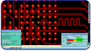
Advanced Software Tools
The use of advanced software tools can dramatically improve the total efficiency of the design and fabrication of HDI PCBs. Designing, simulating, and testing a PCB is an intensive task, and some of these tools enable designers to make the layout more optimal, conduct a signal integrity test, and even simulate what the board will do after being manufactured.
Some important software tools used in HDI PCB design include:
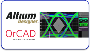
- PCB design software such as Altium Designer and Cadence OrCAD.
- Signal integrity assessment tools.
- Thermal analysis software to integrate heat management into the design.
- These tools help designers to speed up the iterations while still enhancing the design quality.
-
Interdisciplinary Design and Manufacturing Cooperation
Interdisciplinary design and manufacturing cooperation are of great importance in the production flow. The manufacturing engineers should be included in the design of phase one to overcome problems before production starts. This helps to minimize rework, time inefficiencies, and the risk of nonconformity within the project.
It also helps if the DFM issues can be tackled at the design stage, as they would then have to be addressed at a later stage in the process schedule.
-
DFM Compliance
DFM(Design for Manufacture) is defined as a series of activities in a product design process whose main objective is to improve the efficiency of manufacturing processes. Designers can and should follow these DFM rules to ensure efficient and high-quality HDI PCB fabrication.
Some DFM principles are:
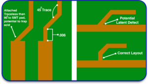
- Making assembly less complicated by eliminating unusual shapes and strict tolerances.
- Whenever possible, use off-the-shelf parts for faster delivery and cheaper prices.
- Trace and via positions should be placed in the optimal routing points to reduce the error rates.
Adhering to DFM regulations provides the manufacturers various advantages like avoiding costly redesigns and making production planning easier.
-
Innovations in Technology in the Mould Making Industry
With the advancement of technology, new methods have been devised for manufacturing HDI PCBs, which have improved the precision and performance of actual HDI PCBs. The following are the most important improvements:
- Laser drilling can create high-precision microvias. Shrinking the drill bits provides greater circuit density, which is necessary for HDI PCBs.
- This technology is also known as 3D printing. With this innovation, PCB designs can be made after scantlings are taken, thereby minimizing material waste. The design freedom provided by additive manufacturing allows for easier manufacture of sophisticated board geometry.
- This technique allows volumetric thick film deposition on HDI PCBs with no metallic traces. It enables the implementation of more complex circuitry while maintaining the performance and reliability standards expected of HDI PCBs.

-
Ongoing Surveillance of the Process
For the manufacturing of the HDI PCB, ongoing surveillance of the process is crucial to ensure smooth operation.
Key parameters that can be monitored in real time, such as temperature profiles during soldering, etching rates during chemical treatment, and automated inspection post-component mounting, allow manufacturers to preemptively discover and address any problems that may arise before the final product quality is compromised.
Continuous monitoring of each phase allows the manufacturers to take corrective actions immediately, reducing defects and improving the overall quality of the product.
-
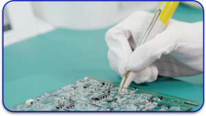
Control and Examination of Quality
Controlling the quality at every procedure of the manufacturing process of the HDI PCB is extremely important. There should be extensive testing procedures to be done so that signal integrity, electrical performance, and reliability for the current use can be established. Some of the testing methods include:
- Automated Optical Inspection: This technique uses specific cameras and software to observe the PCB and its defects, ensuring that it meets the board’s design specifications.
- Electrical Testing – Assures signal interconnections on the PCB are in order.
- Thermal Testing – Checks the performance of the PCB with respect to heat during normal operating conditions.
By enforcing quality control, each HDI PCB can be assured to function and provide the claimed reliability.
The process of designing and manufacturing HDI PCBs is complex and requires accuracy, thoroughness, and contemporary technologies. However, these HDI PCBW can be manufactured cost-effectively with high quality by improving the layout design with respect to the best methodologies and DFM principles, using modern software systems, and cooperating between the organization’s design and manufacturing departments.
Adhering to the methodologies highlighted will promote efficiency throughout the entire manufacturing process, allowing PCB board manufacturers to focus on the bottom line and the reliability and effectiveness of the final products.
Domestic and International Markets for PCBs tend to evolve, so manufacturers must keep abreast of new developments within the manufacturing sector.


