The desire for a more holistic approach regarding the scale and functionality of devices is evident and very much alive, from mobile phones to medical devices and everything in between.
Within the field of electronics, miniaturization has always been at the forefront of innovation, with HDI PCBs being a key contributor to modern technology’s compact designs.
The importance of custom PCB manufacturers being ahead of technological advancements in the market cannot be understated.
Effects of Miniaturization on the HDI PCB Technology Development
In HDI PCB manufacturing, miniaturization involves enhancing the PCB’s performance while reducing its size and the physical space required to accommodate the components.
Innovation is evident in the challenge of combining a smaller form factor with heightened complexity.
Custom PCB manufacturers that have or can develop the capabilities to understand and take advantage of these trends are not only able to provide products that satisfy the current needs of the market but also lead in the industry’s new levels of design leadership.
-
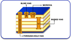
Advanced Vias for the HDI PCB Development
Microvias are the primary elements for the miniaturization of the HDI PCBs. The fabrication of micro vias made it possible to manufacture small, dense vias in PCBs by using laser drilling techniques that permit greater routing density.
This is highly desirable in small, compact systems where space is limited. The addition of blind and buried vias reduces the size of the board while increasing the functionality of the board. The new technologies via design are essential for reducing the dimensions of the PCB without losing or improving the performance.
-
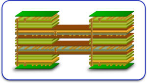
Embedding Components and Stacking of Layers
The conventional method of layering copper foil is now being replaced by new technologies that permit the embedding of components in the layers of the PCB. This new method saves space and enhances electrical performance by reducing signal interference.
Packed into a compact space, multilayer HDI PCBs can have more components without adding to their physical sizes. This also means that for a custom PCB manufacturer, there is increased design freedom when boards have to be space-constrained yet highly efficient.
-
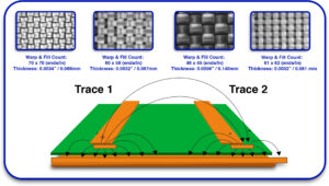
Innovations In Materials
The evolution of PCB materials contributes significantly to miniaturization. The use of high-frequency substrates, low-loss laminates, and other flexible materials makes it possible to achieve better performance in smaller packages.
These materials maintain signal integrity and improve the thermal performance of the boards while ensuring that they are lightweight and compact. The incorporation of polyimide films and ceramic-filled materials improves the durability and flexibility of the PCBs, allowing for more dynamic uses, such as in wearables or automotive applications.
-
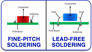
Enhanced Soldering Methodologies
The smaller the components become, the more complex the soldering process is. More modern methods, such as lead-free soldering and fine-pitch soldering, offer solutions to the new problems of miniature components.
These techniques allow good connections to be made without damaging the PCB’s performance. A custom PCB manufacturer must adopt these soldering techniques in order to guarantee the performance and quality of HDI PCBs with high-density designs.
-
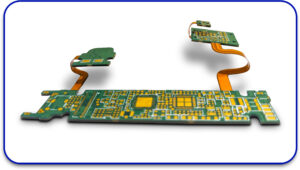
Combination With Flexible PCBs
Perhaps the most interesting area of development in HDI PCB technology is the merger of rigid and flexible PCB technologies, resulting in rigid-flex PCBs. These offer the advantages of both the strength and stability of rigid boards and the pliability of flexible boards.
Rigid-flex PCBs enable the design of small, lightweight, and dependable devices that can bend and flex without causing damage to the internal structure. This is very important in the fields of wearable electronics, medical devices, and consumer electronics, as the devices have to be durable and space optimized.
-
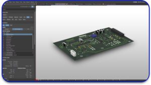
Automated Design and Manufacturing Tools
To keep pace with the rising intricacy and HDI PCB Manufacturing, manufacturers are embracing new design software coupled with automated design and production equipment. Such procedures facilitate the design process, which, in return, improves the speed of prototyping and production.
Applying 3D modeling, signal integrity analysis, and automated optical inspection (AOI) enables manufacturers to improve the design of HDI PCBs, which, in turn, results in high quality, reliability, and compactness of the final products.
How Miniaturization Enhances HDI PCB Applications
The advancing trend of miniaturization in HDI PCBs provides new opportunities for different economic sectors.
The ability to build smaller, more powerful, and efficient PCBs makes it possible to produce a variety of products that could previously not be manufactured. Some of these key applications are:
- Wearable Technology: With the popularization of devices such as smartwatches and fitness trackers comes the demand for miniaturized PCBs. HDI PCBs are preferred since they facilitate the integration of small but powerful circuits that can fit into the wearable devices’ compact form factors.
- Medical Devices: From implantable devices to portable diagnostic tools, miniaturized HDI PCBs are critical to advancing medical technology. These boards provide the reliability and precision required for life-saving applications.
- Consumer Electronics: The market for lighter and more powerful devices, such as smartphones, tablets, and laptops, is now gravitating towards the miniaturization of components, driven by the ongoing trend of thinner devices.
- Automotive Industry: Space limitations and performance requirements have led to the application of HDI PCBs in automotive electronics, such as autonomous vehicles, infotainment systems, and safety systems.
Developments in the miniaturization of electronic components have had a positive impact on the electronic industry, particularly in the possibilities opened by HDI PCB advancements.
As a custom PCB manufacturer, adopting these new developments is indispensable for the production of high-quality, highly dependable, and compact devices. Moving forward, the application of new approaches via design, material selection, structural design, and component integration aids in the advancement of electronic device boundaries.
At Blind Buried Circuits, we strive to be the leader in the HDI PCB market. Whether you need custom answers for your forthcoming project or wish to exploit the latest progress in component miniaturization, we are ready for you. Contact us to discuss how to use state-of-the-art HDI PCB technology to achieve your goal.


