It is noticed that custom PCB manufacturing has grown tremendously in demand in recent years. Precision and efficiency are now of the utmost importance. One area that designers tend to ignore is impedance. The efficiency and reliability of a printed circuit board are highly dependent on impedance and its impacts on performance.
This blog will discuss the effect of impedance on circuit performance.
Defining Impedance
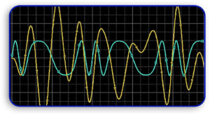
In simple terms, impedance is the total opposition that an AC circuit offers to the flow of alternating current. Unlike pure resistance, impedance includes both resistance (R) and reactance (X). Resistance opposes the flow of current regardless of frequency, while reactance arises due to the presence of inductors and capacitors in the circuit and varies with frequency.
Impedance is represented by the symbol Z and is measured in ohms (Ω), just like resistance. The key difference between impedance and resistance is that impedance applies to alternating current (AC) circuits and takes into account both the energy stored and dissipated in the circuit. Reactance is further divided into two types:
- Inductive Reactance (XL): Caused by inductors, which oppose changes in current.
- Capacitive Reactance (XC): Caused by capacitors, which oppose changes in voltage.
The impedance equation in an AC circuit is:
Z = √(R² + (XL – XC)²)
The physical structure of the circuit, along with the frequency of the AC signal, plays a major role in determining the overall impedance. Understanding and measuring impedance accurately is crucial for improving circuit efficiency, as it helps minimize energy loss and optimize performance.
Impedance and how it impacts the efficiency of a circuit in Custom PCB manufacturing
1. Signal Integrity
A reduction in the quality of a signal can occur due to data errors caused by signal reflection, which is a result of an impedance mismatch. This concern is very important in high-speed telecommunications, data processing, and automotive circuits.
 2. Power Efficiency
Power losses are a result of insufficient impedance control. This unnecessary expense may lead to excessive heat and energy use and as a result, shorten the life span of components.
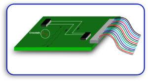
3. Crosstalk and Electromagnetic Interference (EMI)
Excessive crosstalk between adjacent traces and EMI can result from high impedance values. These effects create a need for better impedance control.
4. Component Performance
Many components, including antennas and RF circuits, require matching loads to achieve peak performance. Gaps from paralleled loads can dramatically change how devices work.
Impedance in Blind and Buried Via Circuits
Blind and buried vias are used in multilayer PCBs and are important for miniaturized and powerful devices. They make connections between different layers of a circuit without having to go through the entire board which saves space and enhances signal routing.
Nonetheless, the location and the arrangement of these vias need to be chosen with care as they may alter the impedance of the circuit. These parameters as well as trace widths have to be optimized to meet the dielectric requirements in these types of circuits.
For Impedance Measurement in Customized PCB Design
There are several ways to take and check the measurements of impedance in Custom PCB manufacturing such as:
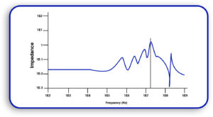
1. Time Domain Reflectometry (TDR) – TDR is one of the most commonly used techniques of taking impedance measurements. It operates by sending a sharp pulse down the circuit and receiving and registering the return signals. Even the smallest mismatch of the impedance will result in some reflection of the signal, which TDR should be able to pick and measure.
2. Vector Network Analyzers (VNA) – The impedance measurement of RF circuits is performed with the help of a VNA, which does so by controlling the circuit’s response at different frequencies. This technique is very precise but quite expensive and much more difficult to implement.
3. Software for Impedance Simulations and Calculators – In the design stage, impedance calculators and simulation tools assist in estimating the impedance of traces and vias. They incorporate the impedance equation with the traces structures, material characteristics, and frequency.
4. Testing Prototypes of PCB – In most cases there are additional steps required in custom PCB manufacturing, extensive testing should follow after physical prototyping. The design Ts requirements should also pass with regards to the impedance values.
Most Effective Control over Impedance in PCB Design
1. Use Controlled Impedance Layers – Designate layers for signals of higher frequencies with very controlled impedance levels for signal fidelity.
2. Keep Trace Width and Spacing Constant – Keep the width and spacing of traces uniform to prevent impedance steps.
3. Choose Appropriate Dielectric Materials – Select components that possess stable dielectric constants and lower loss and tangent.
3. Adjust the Design of Vias – Shorten and reduce the most deep and notched vias to reduce impedance level changes.
4. Conduct DFM Analysis – Work with your specialized PCB fabricator on a proper DFM analysis to easily understand the PCB geometry. This helps fix a lot of impedance issues early on in the design stage.
Impedance is a key factor in determining circuit efficiency, especially in AC circuits where both resistance and reactance come into play. Proper impedance management reduces energy loss, improves performance, and ensures reliable functionality. For engineers and businesses working on advanced circuit designs, controlling impedance is essential for achieving optimal results.
Looking for precision in your circuit design? Our Custom PCB manufacturing services at Blind Buried Circuits offer tailored solutions with accurate impedance control, blind and buried vias, and high-performance results. Contact us today to bring your project to life with reliability and efficiency!


