Custom PCB production in the USA is an essential element of any high-end electronics device. From consumer products like smartphones to sophisticated industrial machinery, printed circuit boards (PCBs) are at the heart of numerous applications. Refined design elements in a PCB’s architecture are vital to ensure reliability. One of them is the annular ring design, which plays a substantial role in a board’s durability and overall performance.
In assisting PCB production in the USA, or anywhere else for that matter, it is imperative to know and apply best practices for annular ring design. This article covers the definition, importance, and practical guidelines for designing robust, high-quality PCBs.
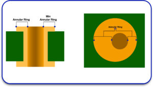
What Is an Annular Ring?
An annular ring is the area of copper that encircles a via or drilled hole in a PCB. This ring serves as a link connecting traces to the various layers of the board, enabling seamless integration of components through electrical signals.
To offer an analogy, it is similar to the edge of a cup. If the edge is excessively thin or not smooth, it can break easily. Likewise, problems of electrical connection failures, tangency, or breakout are associated with insufficiently designed annular rings.
Why Are Annular Rings Important in PCB Design?
Annular rings are critical to achieving a dependable electrical connection between different layers on the PCB. They hold PCB components securely in place through soldering and help reinforce the PCB’s stability.
If the solder mask has an opening diameter that is greater than the barrel height or is not properly aligned with the barrel holes, it can lead to:
– Under-Applied: This is when the copper annular ring does not extend sufficiently, resulting in a weak connection.
– Hooking: This is when the missing annular pad will result in very low-strength connections.
These issues have the potential to increase a circuit’s impedance, which can affect the reliability of the board in question.
Key Design Considerations for Annular Rings
To ensure that the PCB is designed and manufactured correctly, and not easily damaged, specific rules should be followed concerning the construction of annular rings.
Calculation of Annular Ring Width
Use the following formula to determine the dimensions of the annular rings:
Annular Ring Width=Pad Height−Finished Hole Diameter2\text{Annular Ring Width} = \frac{\text{Pad Height} – \text{Finished Hole Diameter}}{2}
For example, assuming:
- Pad Height = 22
- Finished Hole Diameter = 10
The calculation would be:
22−102=6 mils\frac{22 – 10}{2} = 6 \text{ mils}
Introducing the required size eliminates breakouts and ensures good connectivity.
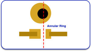
Via Holes Positioning Alignment
The hole used for vias should be drilled directly in the middle of the pad. Loosely obtained holes can increase the probability of tangency or breakouts.
Manufacturer Specifications
Some PCB manufacturers have different criteria for the minimum annular ring size. For example, some recommend a minimum width of a micro via an annular ring of 6 mils to ensure proper PCB production in the USA.
Microteardrop Pads Application
A teardrop pad is obtained by reinforcing the trace polygon copper area with additional copper on the lateral side to the annular ring area. This teardrop shape strengthens the fastening while reducing the chances of failure due to mechanical or thermal stress and other production causes.
Teardrop pads are particularly beneficial for traces of high-density interconnect (HDI) type PCBs that are less than 20 miles wide or with flexible PCBs.
Annular Rings Most Common Problems
Some issues that are likely to occur when the design of the annular ring is not aimed at optimization include:
- Tangency: The copper makes little contact on the edge of the via, thus increasingly compromising the resultant connection.
- Breakouts: Portions of the copper pad are opened, so the reliability of this copper and the circuit will be low.
- Undesirable Annular Rings: Non-alignments or the distribution of heavily dispersed copper can lead to an electrical output that is too different from what was required.
Such problems can be avoided if the marked best practices are adhered to alongside meticulous tolerances for the manufacturing process.
Preventing Breakouts and Enhancing Repeatability
- Increase the Width of Annular Rings: With the proper width, the chance of breakout occurrence is lessened. Try and achieve a minimum of 6-7 mils in width for optimal results.
- Repair Traces With Teardrop Pads: Place more copper at the edge of the trace-via junction connection to strengthen it.
- Drilling Strategy: Find contractors using advanced drilling methods to reduce the chances of misregistration.
The Importance of Better DFM Tools
DFM tools allow you to find issues related to annular rings before going into production. These tools use automation to scan your PCB design files and point out errors that need to be fixed.
Specific DFM tools, for instance, let you set values for minimum annular ring widths, find tangential arcs, and highlight zones where breakouts might happen. Addressing these concerns immediately rather than later can save a lot of time and money from board respins.
Practical Application: Using Proper Annular Rings To Improve PCB Design Reliability
Suppose you’re working on a multi-layer PCB design for an industrial sensor. A number of these boards developed strange intermittent signal issues during production. Upon investigation, you find that the via connection strength is poor as a result of narrow annular rings and slight misalignments.
Further, widening the gaps of the annular rings and subsequently applying teardrop pads increases the reliability of the device and lowers the chances of defects at production. This simple adjustment boosts the product’s performance and longevity.
Considerations To Note for Successful Annular Ring Design
- Talk to Your Manufacturer: Learn what they can do for you and what they won’t be able to accomplish.
- Make Use of DFM Tools: These design tools are valuable in detecting design issues before any expensive production hurdles are encountered.
- Testing and Validation: Confirm that the designed device meets the specifications and functions within the defined limits.
- Using Teardrop Pads: These pads help enhance the strength of the connections, especially in the case of narrow traces and flexible boards.
While not obvious at first glance, proper annular ring design is also a critical success factor in the production of PCBs. Failure to appropriately calculate ring width, center the holes, and drop pads will lead to problems like tangencies and breakouts.
From the USA to overseas, everyone involved in PCB designs and production will benefit from this collection of best practices, knowing that their boards will pass industry standards and be functional. Are you concerned about how your next design will turn out? You can count on Blind Buried Circuits for reliable PCB production in the USA. Contact Blind Buried Circuits for custom-built PCBs that guarantee durability and high quality on every board.


