Designing a printed circuit board (PCB) is a crucial step in developing any electronic device. However, even experienced designers can make mistakes that lead to performance issues, manufacturing defects, or increased production costs. Whether you’re working on custom PCB manufacturing or require fast PCB manufacturing, avoiding PCB design errors is essential to ensure a smooth production process and a reliable final product.
This blog will discuss the most common PCB mistakes, how to identify and prevent them, and best practices for avoiding PCB design issues to improve your layout.
Why Avoiding PCB Design Errors is Important?
Poor PCB design can lead to:
- Electrical failures due to short circuits or incorrect routing.
- Manufacturing delays and costly revisions.
- Signal integrity issues causing unreliable performance.
- Heat management problems that reduce the component lifespan.
- Increased production costs due to inefficient design choices.
By addressing these challenges early in the design phase, you ensure that your custom PCB manufacturing project runs smoothly, reducing rework and improving efficiency.
Top PCB Design Errors and How to Fix Them
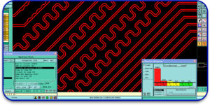
1. Incorrect Trace Width and Spacing
The Problem:
Traces that are too thin may not handle the required current, leading to overheating or even burning out. On the other hand, traces that are too close together increase the risk of short circuits.
How to Fix It:
- Calculate the appropriate trace width using a PCB trace width calculator.
- Follow the recommended spacing guidelines based on voltage levels.
- Use wider traces for high-current paths, especially in fast PCB manufacturing where high-speed signals need controlled impedance.
2. Poor Component Placement
The Problem:
Incorrect component placement can cause routing issues, signal interference, or mechanical constraints.
How to Fix It:
- Place high-speed components near their connectors to minimize signal delay.
- Keep analog and digital components separate to reduce noise.
- Ensure heat-generating components are positioned for effective cooling.
- Maintain enough space for easy soldering and inspection.
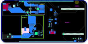
3. Ignoring Power and Ground Planes
The Problem:
Without a proper power and ground structure, your PCB may experience voltage drops, noise interference, and unstable operation.
How to Fix It:
- Use a dedicated ground plane to ensure consistent grounding.
- Place power traces wider than signal traces to handle current loads.
- Minimize the use of multiple small ground traces—use a single, solid plane instead.
- Add decoupling capacitors close to IC power pins to stabilize voltage.
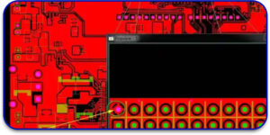
4. Misaligned Drill Holes and Vias
The Problem:
Drill holes that are too small or misaligned can lead to manufacturing defects and component fitting issues.
How to Fix It:
- Verify that via sizes match the PCB manufacturer’s capabilities.
- Ensure vias are correctly aligned with component pads.
- Avoid placing vias too close to solder pads to prevent solder wicking.
5. Not Following Design for Manufacturability (DFM) Guidelines
The Problem:
Ignoring manufacturing constraints can lead to production delays, increased costs, and quality issues.
How to Fix It:
- Follow the PCB board manufacturer’s design guidelines.
- Ensure the board thickness, hole sizes, and copper weights match fabrication requirements.
- Run a Design Rule Check (DRC) before finalizing your layout.
6. Overlooking Signal Integrity Issues
The Problem:
High-speed signals may suffer from reflections, crosstalk, and noise interference, leading to unreliable performance.
How to Fix It:
- Keep high-speed traces as short as possible.
- Route differential pairs close together to maintain signal integrity.
- Use controlled impedance techniques for fast PCB manufacturing.
- Separate high-speed and low-speed signals to avoid interference.
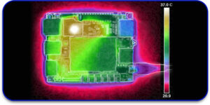
7. Insufficient Thermal Management
The Problem:
Poor heat dissipation can lead to overheating, reducing the lifespan of components and affecting overall performance.
How to Fix It:
- Add thermal vias under heat-generating components.
- Use copper pours to help distribute heat evenly.
- Ensure proper airflow by spacing high-power components appropriately.
 8. Using Incorrect Footprints and Libraries
The Problem:
If the component footprint does not match the actual component dimensions, placement and soldering issues may occur.
How to Fix It:
- Double-check component footprints against the manufacturer’s datasheet.
- Use verified and updated component libraries in your design software.
- Print a 1:1 scale of your PCB layout and place components on it to verify fit.
 9. Overcomplicated Routing
The Problem:
Complex routing with excessive vias and unnecessary layers increases production costs and may introduce signal integrity issues.
How to Fix It:
- Optimize the routing by keeping it as direct as possible.
- Use minimal vias to reduce potential failure points.
- Maintain consistent trace width and spacing for high-frequency signals.
10. Ignoring Testing and Prototyping
The Problem:
Skipping the testing phase increases the risk of unexpected failures once the PCB is in production.
How to Fix It:
- Order a prototype before full-scale custom PCB manufacturing.
- Use test points for debugging and validation.
- Perform functional testing to ensure the board meets design specifications.
Best Practices to Improve Your PCB Layout
1. Plan Your Design Before Starting
- Define clear objectives for your PCB layout.
- Identify critical components and their placement early.
- Consider power distribution and signal integrity from the start.
2. Use Layer Stack-Up Wisely
- Optimize the number of layers to balance cost and performance.
- Use ground planes effectively to reduce EMI and improve signal return paths.
3. Minimize Noise and Interference
- Separate analog and digital sections.
- Shield sensitive traces using ground planes or copper pours.
- Maintain uniform trace spacing to prevent crosstalk.
4. Simplify Manufacturing and Assembly
- Keep a logical component placement to make assembly easier.
- Label all components clearly for efficient assembly and testing.
- Avoid sharp angles in traces, as they can cause etching issues during PCB board assembly manufacturing.
5. Ensure Proper Documentation
- Provide detailed fabrication and assembly drawings.
- Include a Bill of Materials (BOM) with accurate part numbers.
- Document testing and quality control procedures for reference.
6. Use Design Rule Check (DRC) and Electrical Rule Check (ERC)
- Regularly run DRC to catch layout violations.
- Use ERC to verify connectivity and power distribution integrity.
7. Collaborate with Your Manufacturer
- Work closely with your PCB board manufacturer to ensure your design meets production capabilities.
- Share Gerber files, drill files, and specifications before finalizing the design.
- Seek feedback to improve manufacturability and reduce costs.
Avoiding common PCB mistakes is critical for producing a high-quality, reliable, and cost-effective circuit board. By following these best practices, you can enhance your PCB design quality, improve custom PCB manufacturing efficiency, and reduce costly errors in fast PCB manufacturing.
At Blind Buried Circuits, we specialize in providing high-quality PCB board assembly manufacturing services with quick turnaround times. Whether you need a simple prototype or a complex high-speed PCB, our team is ready to assist you. Contact us today to ensure your next PCB design is error-free and optimized for production.


