Modern electronics would not be possible without high-speed PCBs. From computers and communication devices to even medical equipment, these components assist in the seamless transmission and maintenance of data and signals. Poorly designed PCBs will result in signal loss, electromagnetic interference (EMI), and data corruption, all of which will cause massive performance failures.
Understanding the random principles of high-speed PCB design is essential for anyone working on fast PCB design. This article aims to touch on the best practices, challenges, and crucial techniques every designer needs to make sure their PCB is efficient and high-performing. Whether you are an engineer or searching for complete turnkey PCB solutions, these suggestions will assist you in reaching the best outcome possible.
What is High-Speed PCB Design?
High-speed PCB design refers to circuit boards that have issues concerning the integrity of the signals due to the rate of data transmission. Unlike standard PCBs, which can function at lower frequencies, high-speed PCBs require specially designed techniques to avoid issues with signal reflections, noise, and loss.
When a PCB is operating at high speeds, it requires strict adherence to features such as impedance, trace layout, EMI shielding, and control. Neglecting these parameters will lead to signal degradation, which will affect the overall system’s performance.
Obstacles in Fast-paced PCB Design
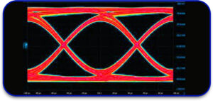
1. Integrity of the Signal
Due to transmission line issues and rapid signals, unwanted noise and signal distortion may occur, resulting in vital information being lost or corrupted.
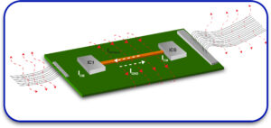
 2. Electromagnetic Interference (EMI)
Near other components, EMI can be harmful. Dynamic signal switching can lead to EMI generation, which can affect the operations within the system.
 3. Inter-relation of Electric Components
Signals reflect discontinuities in the system, which is a result of uncontrolled impedance. The outcome of this is known as signal distortion.
4. Problems Associated with Power Distribution
Poorly designed power delivery networks (PDN) can affect circuit stability by causing voltage changes, also known as fluctuations.
Ways to Handle Fast-paced PCB Design
1. Optimize PCB stackup for high-speed signals:
A fast PCB design greatly depends on how well-engineered the stack-up of the PCB layer is. The optimum structure of the stack-up leads to better impedance control while minimizing EMI.
- Use dedicated ground planes for superior signal return paths.
- Control dielectric thickness to ensure consistency.
- Place ground planes between high-speed signal layers to minimize interference.
2. Set up methods for Controlled Impedance Routing
The changing of impedance results in a controlled area, which enables the hinders of active and passive circuits to be managed. Furthermore, controlled impedance ensures a proper signal flow, and thus, no reflection will occur.
- Use a trace calculator to set impedance, spacing, and width.
- Design analytic pairs, however, with controlled gap spacing.
- Control trace lengths so that they are short enough to prevent signal decay.
3. Limit Stray Capacitance Between Traces
Crosstalk occurs when signals on bordering traces disrupt each other’s signals, causing data corruption.
- Increase the distance between fast signals.
- Use ground planes for separation between signals.
- Route traces on adjacent layers in a perpendicular direction to diminish coupling.
4. Techniques for Proper Circuit Termination
Reflections of signals can interfere with high speed circuits due to a lack of termination. The most common ways to terminate a circuit are:
- Series termination: The impedance at the driver end is matched by a resistor.
- Parallel termination: The stabilizing resistor is found at the receiver side.
- AC termination: A resistor-capacitor combination that restrains the amount of power used.
5. Shorten Tracking and Avoid Sharp Angles
Unwanted noise is a product of long traces combined with sharp angles.
- Traces should be as short as possible.
- Bend at 45 degrees instead of sharp 90-degree angles.
- By using stitching, post holes can be drilled to meet standard impedance control.
6. Create A Robust Power Delivery Network (PDN)
- A good PDN will avoid the steady voltage drop and increase reliability.
- Use wide power traces or dedicated power planes.
- Locate decoupling capacitors next to the power pins.
- Minimize inductive loops to lessen power noise.
Advanced Techniques for High-Speed PCB Design
1. Differential Pair Routine
- Interfaces, including USB, PCIe, and even HDMI, use pairs that are routed to cancel to improve immunity to interference.
- In order to avoid skew, trace lengths should be equal.
- Keep consistent spacing to maintain differential impedance.
- Route differential pairs at equal distances from the reference line.
2. Refrain from Stub Traces
- Stubs are unwanted because of their ability to reflect and distort signals.
- Use via-in-pad technologies for quick and direct routing of signals.
- Refrain from excessive trace branching. .
3. Thermal Management of PCBs
- High-speed circuits must manage heat efficiently.
- Utilize thermal vias for effective cooling.
- Add heatsinks and thermal pads for power components.
- Choose high-Tg materials for PCBs to help with thermal retention.
4. EMI Reduction through Shielding
- High-speed signals also suffer from EMI.
- Shield with grounded copper pours.
- Surround high-speed parts in Faraday cages.
- Grounding and return paths must be provided.
Ways Turnkey PCB Manufacturing Supports High-Speed PCB Design
Turnkey PCB Services guarantees precise fabrication and assembly, which is essential to high-speed PCBs.
Benefits of Turnkey PCB Manufacturing:
- Production occurs at a rapid pace with enhanced efficiency.
- Impedance control ensures expert selection of materials.
- Defect fabrication is minimized, which increases quality.
- Comprehensive testing ensures everything works optimally.
Partnering with a PCB board assembly manufacturing company helps ensure that your high-speed PCB designs have minimal errors when meeting industry standards.
When it comes to rapid PCB design, signal integrity, impedance control, EMI mitigation, and thermal management must be treated with utmost caution. Following best practices will guarantee quick design cycles, optimal performance, and low interference. At Blind Buried Circuits, we provide full turnkey PCB services and electronic assembly manufacturing to ensure your high-speed PCB design meets industry requirements. We are ready to help whether you are looking for professional help or wish to outsource the entire project. Reach out to us today to bring your high-speed PCB project to life!


