When designing a printed circuit board (PCB), engineers often focus on selecting the right components and optimizing the layout. However, applying network theory to PCB circuit design can significantly improve signal integrity, power distribution, and overall performance.
Whether you’re a PCB board manufacturer or an electronics designer, understanding how theory network principles apply to PCB circuits is essential. Concepts like linear networks, electrical circuit topologies, and network circuit analysis can help you create efficient, high-performance PCBs for a wide range of applications. This blog will discuss how network theory applies to PCB circuit design and how you can use it to optimize custom PCB production.
What is Network Theory in PCB Design?
Network theory is a branch of electrical engineering that focuses on analyzing and designing interconnected electrical components. It provides a structured approach to understanding how signals, power, and currents flow through a circuit.
- In PCB manufacturing, network theory helps designers:
- Reduce signal loss and distortion.
- Improve power distribution for stable operation.
- Enhance circuit reliability and efficiency.
- Optimize component placement for better performance.
By applying network circuits principles, PCB manufacturers can produce highly reliable, high-speed, and low-noise PCBs.
Key Concepts of Network Theory for PCB Design
1. Linear Networks vs. Nonlinear Networks
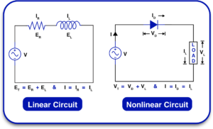
A linear network follows Ohm’s Law, meaning its resistance, capacitance, and inductance remain constant regardless of applied voltage or current. These networks are easier to analyze using Kirchhoff’s Laws and Thevenin’s Theorem.
On the other hand, nonlinear networks have components like diodes and transistors that introduce voltage-dependent changes, making them more complex.
How This Applies to PCBs:
- Linear networks ensure consistent and predictable performance, making them ideal for signal processing and analog circuits.
- Nonlinear networks are necessary for power regulation and switching applications in high-speed digital circuits.
2. Topology in Electrical Circuits
Topology in electrical circuits refers to the physical and logical arrangement of components in a circuit. The choice of topology affects how signals travel, how power is distributed, and how interference is managed.
Common PCB Topologies Include:
- Series Topology: Components are connected end-to-end, commonly used in LED lighting circuits.
- Parallel Topology: Components share the same voltage, ideal for power distribution networks.
- Star Topology: Signals travel from a central point, reducing cross-talk and noise in high-speed PCBs.
- Mesh Topology: Multiple interconnections improve fault tolerance in critical applications.
Choosing the right topology ensures that signal transmission remains stable, and power distribution is efficient.
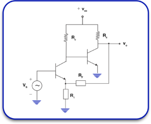
3. Impedance Matching and Network Circuits
In high-frequency PCB design, impedance mismatches can cause signal reflections and power loss. Network circuits help mitigate these issues by optimizing trace widths, terminations, and grounding.
- Key Techniques for Impedance Matching:
- Use of Transmission Lines: Ensures proper signal travel in RF and high-speed circuits.
- Resistive Termination: Absorbs reflected signals in high-frequency networks.
- Stub Matching Networks: Improves signal integrity in antenna circuits.
PCB board manufacturers use network theory principles to optimize impedance matching, ensuring efficient energy transfer in high-speed circuits.
Applying Network Theory to Improve PCB Performance
1. Signal Integrity Optimization
Network theory helps improve signal integrity by minimizing:
- Reflection Losses: Ensuring signals reach their destination without bouncing back.
- Crosstalk: Reducing interference between adjacent traces.
- Voltage Drop: Maintaining steady signal voltage levels.
Best Practices:
- Shorten trace lengths to prevent attenuation.
- Use controlled impedance routing in high-frequency designs.
- Apply proper grounding techniques to reduce noise.
2. Power Distribution Networks (PDN)
Power stability is critical for a PCB’s performance. Poor power distribution leads to voltage fluctuations, signal noise, and component failure.
How Network Theory Helps:
- Star Grounding: Prevents ground loops in multi-layer PCBs.
- Decoupling Capacitors: Filters out noise and stabilizes voltage levels.
- Optimized Via Placement: Ensures low-resistance paths for power flow.
A well-designed PDN ensures reliable power delivery, reducing noise and improving overall PCB performance.
3. Reducing EMI and Noise in PCB Networks
Electromagnetic interference (EMI) can degrade performance in sensitive circuits.
Using Network Theory to Reduce EMI:
- Shielding Techniques: Minimizes external interference.
- Differential Signaling: Reduces noise in high-speed data lines.
- Proper Trace Spacing: Prevents coupling between signals.
By applying network theory, designers can ensure low-noise, interference-free PCB operation.
4. Optimizing PCB Layout with Network Theory
Efficient PCB layouts enhance performance and manufacturability.
Key Considerations:
- Component Placement: High-speed components should be close to power sources.
- Routing Strategy: Avoid sharp trace bends to reduce resistance.
- Thermal Management: Use copper pours to dissipate heat efficiently.
Applying network circuits principles results in compact, power-efficient PCBs with better longevity.
Choosing the Right PCB Manufacturer for Network-Optimized Designs
To ensure high-performance PCBs, working with an experienced PCB manufacturer is essential.
What to Look for in a PCB Manufacturer?
- Expertise in custom PCB production.
- Knowledge of network theory applications in PCBs.
- Ability to fabricate high-speed, low-noise circuits.
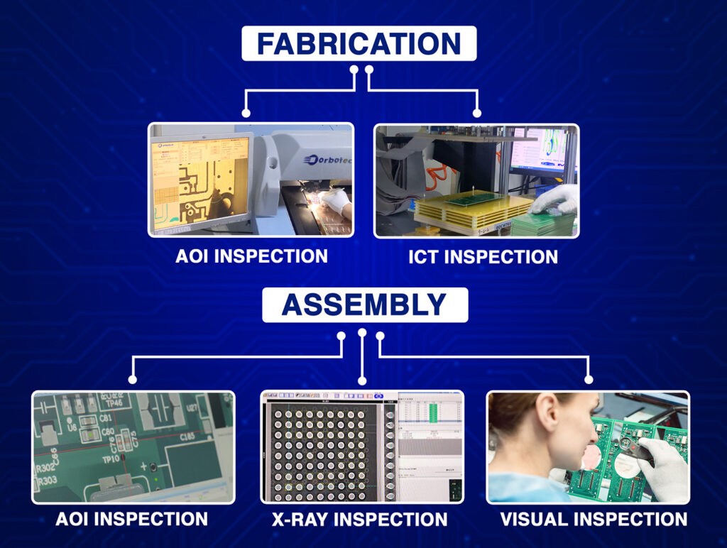
- Advanced manufacturing and testing capabilities.
A well-established PCB board manufacturer will help you implement network-based optimizations for superior performance.
Network Theory is the Key to High-Performance PCBs
By applying network theory principles, PCB designers can improve circuit stability, reduce noise, optimize power distribution, and enhance signal integrity.
Understanding concepts like linear networks, electrical circuit topologies, and network circuits helps ensure that PCBs perform at their best. Whether you’re working on high-speed digital designs, RF circuits, or power electronics, network theory is a powerful tool for custom PCB production. If you’re looking for a reliable PCB manufacturer who understands network-based design optimizations, contact Blind Buried Circuits today! We specialize in high-performance PCB production to help you build the best network-optimized PCBs.

