If you have ever worked with high-speed PCB designs, you know how important it is to maintain strong signal integrity. One of the biggest challenges is signal attenuation, which refers to the gradual weakening of a signal as it travels through a circuit. If not properly managed, attenuated signals can lead to communication errors, timing issues, and overall performance failures. For any PCB manufacturer, ensuring that PCB board assembly manufacturing processes optimize signal transmission is essential for creating reliable, high-performance products. Whether you are working with flexible PCB fabrication or rigid PCBs, poor signal integrity can lead to wave attenuation and networking failures in high-frequency applications.
This blog explains why signal attenuation happens, how it affects performance, and the best strategies to reduce it in your high-speed PCB designs.
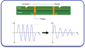
Understanding Signal Attenuation in PCB Design
What is Signal Attenuation?
Signal attenuation is the loss of signal strength as it moves through a PCB trace, connector, or transmission line. In high-speed circuits, attenuation can cause data corruption, transmission failures, and reduced device performance.
Common Causes of Signal Attenuation
Several factors contribute to signal attenuation in PCBs, including:
- Resistive Losses: Electrical resistance in PCB traces causes energy dissipation as heat.
- Dielectric Losses: The PCB material absorbs signal energy, leading to a weaker signal.
- Impedance Mismatch: Sudden changes in impedance lead to reflections and energy loss.
- Crosstalk and Noise: Interference from adjacent traces or components degrades the signal quality.
By understanding these factors, you can design your PCB to minimize signal loss and achieve better transmission efficiency.
Effects of Signal Attenuation on PCB Performance
When designing high-speed PCBs, controlling signal attenuation is critical for ensuring reliable communication. Poorly managed attenuation can result in:
- Distorted Signals: Weak signals may lead to misinterpretation of data.
- Slower Data Speeds: High attenuation can reduce transmission speed and efficiency.
- Increased Error Rates: A weak signal is more likely to be affected by noise and interference.
- Reduced PCB Reliability: Excessive signal loss can shorten the operational lifespan of a PCB.
For industries that rely on high-speed data transmission, such as telecommunications, aerospace, and automotive electronics, minimizing signal attenuation is a top priority.
Best Practices to Reduce Signal Attenuation in High-Speed PCBs
1. Choose Low-Loss PCB Materials
The material used in PCB manufacturing technology plays a significant role in reducing signal attenuation.
Recommended Materials for Low Signal Loss
- FR-4: Commonly used but has moderate signal loss at high frequencies.
- Polyimide (for Flex PCBs): Offers good dielectric properties and flexibility.
- PTFE (Teflon-based PCBs): Ideal for RF and microwave applications due to low dielectric loss.
- Rogers Materials: Known for superior performance in high-frequency circuits.
Choosing the right PCB material is crucial for mitigating outgassing in PCBs and ensuring long-term reliability.
2. Optimize PCB Trace Design
PCB traces act as transmission lines, and their design can significantly impact signal attenuation.
Best Practices for PCB Trace Design
- Use Wider Traces: Helps reduce resistive losses by lowering resistance.
- Shorten Signal Paths: Reduces overall attenuation by minimizing the distance signals travel.
- Optimize Trace Spacing: Prevents crosstalk and interference between signals.
- Implement Microstrip and Stripline Designs: These techniques improve controlled impedance and signal quality.
An optimized PCB layout is essential for reducing wave attenuation and improving high-speed performance.
3. Maintain Proper Impedance Matching
Impedance mismatches cause signal reflections, leading to energy loss and signal distortion.
How to Ensure Proper Impedance Matching
- Use Controlled Impedance Design to maintain consistent signal paths.
- Include Termination Resistors to absorb reflections.
- Simulate Circuit Behavior to analyze impedance issues before manufacturing.
By managing impedance control, you can improve attenuation networking and enhance PCB signal integrity.
4. Use Differential Pair Routing for High-Speed Signals
Differential routing helps cancel out noise and reduces signal attenuation in high-speed circuits.
Benefits of Differential Pairs
- Minimizes Electromagnetic Interference (EMI).
- Enhances Signal Integrity by balancing positive and negative signals.
- Prevents Data Corruption in high-speed communication applications.
Differential pairs are commonly used in IoT PCB design and RF circuit layouts.
5. Design an Efficient PCB Layer Stackup
A well-structured PCB stackup helps minimize dielectric and resistive losses.
Best Practices for Layer Stackup
- Use Ground Planes close to signal layers to reduce loop inductance.
- Choose the Right Prepreg Materials for controlled impedance.
- Optimize Layer Thickness to maintain consistent transmission paths.
An optimized stack-up design supports high-speed PCB fabrication and ensures minimal signal degradation.
6. Reduce PCB Crosstalk and Noise
Crosstalk and interference are major contributors to signal attenuation in high-speed circuits.
How to Reduce Crosstalk
- Increase Trace Separation: Reduces signal coupling between adjacent traces.
- Use Ground Shields: Helps isolate sensitive signal paths.
- Implement Proper Termination Methods: Controls unwanted reflections and noise.
By reducing crosstalk, your PCB will maintain stronger signal integrity and better overall performance.
7. Optimize Connector and Via Designs
Connectors and vias introduce discontinuities that can lead to signal degradation.
Ways to Minimize Signal Loss in Connectors and Vias
- Use Low-Inductance Vias to maintain signal continuity.
- Avoid Excessive Via Transitions to prevent impedance mismatches.
- Choose High-Quality Connectors to reduce insertion loss.
Proper via and connector design ensures consistent signal transmission in high-speed PCBs.
The Future of High-Speed PCB Design and Attenuation Control
With the increasing demand for 5G, IoT, and high-speed computing, minimizing attenuation is more important than ever.
Emerging Trends in PCB Signal Integrity
- Advanced Dielectric Materials to reduce signal loss.
- AI-based PCB Design Optimization for better high-speed performance.
- Ultra-Fine Line Manufacturing to improve precision and signal transmission.
As PCB manufacturing technology advances, new solutions will continue to enhance signal integrity and reduce attenuation.
Controlling signal attenuation is essential for high-speed PCB performance. By using low-loss materials, optimized trace designs, impedance matching, and proper stackup techniques, you can minimize signal loss and ensure reliable communication. For high-performance PCB board assembly manufacturing, partnering with an experienced PCB manufacturer like Blind Buried Circuits ensures that your designs meet the highest quality standards. Contact us today to optimize your high-speed PCB projects.

