When you’re working on a complex electronic device, the printed circuit board (PCB) inside is likely doing a lot more than it looks. Today’s compact gadgets need advanced boards that can handle tight spaces, high speeds, and firm performance. That’s where multilayer HDI-PCBs come in. To build those boards right, the sequential lamination process is key.
If you’re planning a project or choosing a PCB manufacturer, understanding sequential lamination will help you make better choices, save time, and avoid problems later. Let’s break it down.
What Is Sequential Lamination in PCB Production?
Sequential lamination is a step-by-step layering method used to build complex multilayer PCBs, especially high-density interconnect (HDI-PCBs). Instead of stacking all layers at once, the PCB manufacturer presses a few layers at a time. Then, they drill and plate them before adding more layers.
This process repeats until the whole board is ready. It allows for a more accurate high-density PCB design with smaller vias and tighter spacing.
Why Do HDI PCBs Need Sequential Lamination?
HDI PCBs use fragile traces, microvias, and stacked structures. You’ll find them in smartphones, aerospace tools, medical devices, and any product that needs high performance in a small space.
These boards often use:
- High-density PCB connectors
- Blind and buried vias
- Laser-drilled micro vias
- Complex signal paths
To create all of that without errors, you need to build the board layer by layer. That’s precisely what the sequential lamination PCB method allows.
Benefits of the Sequential Lamination Process
1. Better Layer Alignment
Each layer needs to be perfectly aligned. The sequential lamination process gives the manufacturer better control. It reduces the risk of misalignment, which is common when stacking many layers at once.
2. Supports Advanced Via Structures
Many HDI-PCBs use stacked or staggered vias to save space and improve connectivity. These features can’t be built in one press cycle. You need multiple lamination steps to add each set of vias correctly.
3. Boosts Electrical Performance
With better alignment and shorter connections between components, your signals move faster and more reliably. That matters if you’re working with fast processors or radio frequencies.
4. Reduces Space
By using high density PCB connectors and tight layouts, designers can shrink the size of the board while keeping or even improving performance. Sequential lamination is the only way to make this possible at scale.
Where You’ll Find HDI PCBs With Sequential Lamination
If you’re holding a modern phone, tablet, or smartwatch, chances are it’s powered by a multilayer HDI-PCB. But it’s not just in consumer electronics.
Here are more industries that rely on this:
- Medical devices with small, high-speed boards
- Automotive systems with compact sensors and infotainment
- Telecom gear like base stations and routers
- Military and aerospace electronics that must save space and stay reliable
Every PCB manufacturing company building HDI boards uses sequential lamination to meet these design needs.
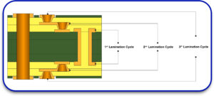
What Happens During the Sequential Lamination Process?
Let’s walk through a simple version of how this works.
Step 1: Create Core Layers
The PCB manufacturer starts by building a few core layers. These often have copper patterns already etched.
Step 2: Laminate First Stack
These cores are laminated under heat and pressure. Think of it like pressing a sandwich together so all the layers bond well.
Step 3: Drill and Plate Vias
After the first press, the board is drilled, and the holes are plated. This connects the layers electrically.
Step 4: Add More Layers
Once the first set is solid, another few layers are stacked on top. Then they’re pressed again. The sequential lamination PCB method repeats this process until all layers are in place.
Step 5: Final Drilling and Coating
In the last steps, the board gets its outer layers, more via holes, and finishes like gold plating or solder masks.
Why This Process Requires a Skilled Manufacturer?
Not every pcb manufacturing company can handle HDI boards with sequential lamination. It needs high-precision equipment, clean environments, and expert handling at each stage.
When choosing a PCB board manufacturer, look for these signs:
- Do they have experience with HDI-PCBs?
- Can they share examples of PCB production USA for high-density applications?
- Do they follow strict quality checks at each lamination step?
Working with a trusted partner helps you avoid delays, defects, and wasted money.
What Could Go Wrong Without Sequential Lamination?
Skipping or poorly performing this process can lead to:
- Layer misalignment
- Via failures or shorts
- Warping or bending
- Poor signal integrity
- Unstable high-speed performance
In short, without proper lamination, your HDI design may look fine on paper but fail in real use. If your goal is a compact, powerful board, sequential lamination isn’t optional.
How Sequential Lamination Supports Design Freedom?
As a designer, you may want to fit more parts into less space or add features without making the board bigger. With the help of sequential lamination PCB methods, you can:
- Use more layers without adding thickness
- Add stacked vias for denser connections
- Match complex footprints for custom chips or connectors
- Optimize signal paths for speed and power
This process gives you more control to build smarter boards that still fit in tiny packages.
What Should You Ask Your PCB Manufacturer?
When you’re ready to order your boards, especially if you’re sourcing from PCB Production USA, ask the right questions:
- Do you offer sequential lamination for HDI-PCBs?
- What is your yield rate for multi-lamination jobs?
- What surface finishes and via options do you support?
- Can you share your lamination and inspection process?
These details can make or break your project, especially if you’re building for industries where reliability is everything.
Final Thoughts
Sequential lamination is the backbone of successful high-density PCB design. Without it, your HDI board could fall short in performance, quality, or size. Whether you’re working with a local PCB manufacturing company or ordering from a PCB production USA vendor, you need to make sure they understand and can deliver on this process.
Don’t just focus on cost or delivery time. A skilled PCB board manufacturer with proper experience in sequential lamination PCB production will save you trouble and give you better results in the long run.
So, if your project depends on compact, high-speed, and multi-layer designs, make sequential lamination part of your plan from the very beginning.


