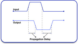
A device’s performance often hinges not just on its components but also on how those components are connected, specifically, how signals travel between them on a printed circuit board (PCB). One of the most critical parameters that PCB designers must account for, particularly in high-speed and radio-frequency (RF) applications, is signal propagation delay.
As previously discussed, it is a measurement of the time an electrical signal takes to move from one geographical point to another along a transmission line. In circuit theory in its simplest forms, instantaneous flow is often assumed and is not the case in reality. Signals move at finite speeds which is determined by the physical and electrical properties of the board.
Now let’s look into the calculation of propagation delay as well as as understanding how it can induce issues such as integrity, timing, performance malfunctions in signals of intricate electronic systems – which Blind Buried Circuits aims to resolve through meticulous engineering alongside sophisticated PCB layout techniques.
Understanding What is Signal Propagation Delay,
On a fundamental level, signal propagation delay is the inverse of the signal speed the medium. The dielectric materials in the circuit boards are slower than light in a vacuum. Primary contributors to the signal speed includes the dielectric constant (Dk) of its substrate, geometry of the trace (width, height, and distance to the reference plane), and whether the trace is microstrip, stripline, or a differential pair.
For instance, a typical signal travelling through a 50 ohm microstrip over a dielectric with Dk ≈ 4 has a SPD of approximately 150 picoseconds per inch while a stripline would be closer to having a delay of 171 ps/inch because of the differences in electromagnet field distribution. These delays can be achieved in a lower absolute terms, but would be critical in high-speed or high-frequency designs.
Why It Matters: The Leading Uses in PCB Layout Design
1.Timing Precision of High-Speed Digital Interfaces
In high-speed digital systems such as DDR memories, PCIe buses, and serial data links, signals must reach destinations within specified deadlines. These windows shrink as clock rates increase. In fast asynchronous circuits, if two signals that are intended to reach a destination simultaneously arrive at an endpoint slightly out of order, it could bring about timing violations and data corruption.
For the case of timing mismatches, the most common method is trace length tuning. Designers apply step propagation delay to determine how much greater or lesser a trace ought to be in order to time-align signals. Take the parallel bus for example, if two traces are unequal in length, the resulting timing skew could cause data to be incorrectly captured. Designers can convert time mismatches to physical length mismatches which can be untangled through timed routing, known signal propagation delay helps out with the timing mismatches.
2. Preserving Signal Integrity in Differential Pairs
USB, HDMI, and LVDS interfaces use differential signalling because it is fast and good at resisting noise. the advantage will only apply if the phase and timing alignment between the two traces in each pair is tight.
Negative and positive traces as signals differ in terms of time, known as intra-pair skew, may unbalance the signal and result in increasing electromagnetic radiation while lowering the signal’s quality. This concern is critical when placing routing differential pairs on different layers or through holes. With a signal’s propagation delay, the signal delay time, as a tuning parameter, they ensure equal electrical lengths for all pairs regardless of how rigid their paths are.
3. Phase Control in RF and Microwave Systems
Consistency in the value of phase shifts and timing in RF applications takes priority over phase shifts alone. The trace distance to which a signal travels in a PCB is a function of its SPD (Speed Propagation Delay), which in turn is influenced by the board’s design. Any delay which is incurred during signal transmission will have substantial ramifications in functionality, particularly in the presence of antennas, filters, and resonators.
Consider phased array antennas for instance. They experience use in radar, satellite communications, and 5G networks. It is important for multiple antennas to be able to either transmit or receive signals in a pre-defined, phase dependent order. Signals with incorrect phase relationships due to different trace lengths or propagation speeds result in beampatterns with misdirected signals and reduced gain. Their solution is to phase align feedlines and adjust delays using precise calculations which ensure phase accuracy, all of which relies on knowing the SPD.
4. Input Reflection and Reflection Analysis
Looking at the way a transmission line links up a signal source to a load, signal propagation delay also affects matching on these impedances. Interference from reflections degrades performance and is caused by mismatched impedances along the transmission path.
Any section of a transmission line has an input impedance that changes based on the electrical length of the line and signal propagation delay. It is modeled as a function of delay and impedance, allowing forecasters to make predictions on frequency reflection significance to determine termination or matching network placement.
Tools and Automations
Many modern Automated design systems work with PCBs and provide features that add measurement materials and geometry which results in trace delay. Instant verification for delay matching, differential pair adjustment, and impedance setting is available. Altium designer for instance has the ability to notify users as they design when time differences exceed allowed timings and has the ability to propose and perform routing corrections on his behalf.
In some cases, the calculation of the signal propagation delay requires specific simulation tools or field solvers, particularly with sophisticated transmission line configurations such as coplanar waveguides or when considering fibre weave complications with PCB materials that introduce signal skews and delays during transmission.
Companies like Blind Buried Circuits, specialising in PCB assembly USA, offer the advantage of faster turnaround times, better communication, and compliance with local manufacturing standards. Whether you’re developing prototypes or scaling to full production, seamless integration between PCB manufacturing, assembly, and testing processes is key. Leading PCB board assembly manufacturing services combine advanced equipment, skilled technicians, and rigorous quality control to deliver high-performance circuit boards tailored to your exact specifications.
Conclusion
Aside from being an academic subject, the concept of signal propagation delay is very much a reality in PCB design impacting data and RF performance. Maintaining bit-aligned data transfers in high-speed digital systems or ensuring phase coherent signals in radar antenna arrays depends on the effective control and understanding of signal propagation delays essential for efficient, dependable electronics systems.
The importance of signal propagation delay in PCB design will increase as systems continue to evolve in speed and complexity. Mastering this parameter allows designers to maximize performance while sustaining signal integrity, timing precision, and reliability of the system. In custom PCB production, choosing a reliable partner like Blind Buried Circuits helps guarantee quality and performance.


