Impedance control is one of the most critical impedances that affects a PCB manufacturing assembly as it dramatically influences the quality of high-speed circuits. If it is unchecked, signal degradation may occur which results in reflection, power loss, and unreliable circuitry.
Understanding impedance matching, why PCB impedance is essential, and how to control it can be difficult for novices. However, given adequate techniques and understanding, it is possible to design and manufacture PCBs with precise signal accuracy and proper efficiency. In the following sections of this article, we will cover the definition of control, the reasons why control is essential, and how to add control to your PCB assembly service so that a dependable, high-performance board is produced.
What is Impedance Control in PCB Design?
Impedance is defined as the degree of opposition a circuit presents to the flow of an alternating current (AC). It is expressed in ohm( Ω) units, and depending on factors, it can be capacitance, resistance, or inductance; it can change. During PCB manufacturing assembly, impedance control ensures that certain signals maintain their integrity while traveling via traces. Improper impedance matching may result in distortion or reflection of the signals, especially for high-frequency circuits, which may lead to failures.
Why Is Impedance Control Important?
Impedance control is the silken thread that weaves through the fabric of modern PCB designs, especially for high-speed digital and RF circuits. Here’s why:
1.Keeps Reflection Incheck
If the impedance is not matched appropriately, a portion of the signal is reflected rather than transmitted, which can cause interference and unreliable circuit behavior.
2. Boosts Signal Quality
Controlled impedance reduces signal loss and distortion protecting the well functioning of the circuit.
3. Minimization of Electromagnetic Interference (EMI)
Controlled impedance mitigates excessive EMI, which could affect nearby circuits, which is non-compliance with industry standards.
4. Better Reliability of PCB
These designs reduce unwanted noise and provide stabilized operational circuits, which are needed in the medical, automotive, and aerospace industries.
Things That Impact the Impedance of PCB
There are a couple of factors that affect impedance matching in PCBs. These factors are critical for controlled impedance designs:
1. Width and Thickness of Trace
These parameters of the copper traces straightforwardly impact their resistance and inductance. Wider traces typically have lower impedance.
2. Dielectric material of PCB
The type of dielectric material (an insulator layer) used in the PCB affects capacitance and impedance. Different materials, such as FR4, Rogers, and Teflon, carry different dielectric constants that influence signal transmission.
3. Distance Between Traces and Ground Planes
In the PCB assembly design, a trace nearer to a reference plane (ground or power) has a lower impedance. Designers have to carefully manage the impedance change layer stack-ups within the target impedance.
4. Signal Frequency
For signals of higher frequencies, impedance control becomes more demanding due to the increased possibility that part of the signal will be reflected or lost.
5. PCB Layer Stack-Up
Impedance affects multi-circuit boards since the number of multilayer boards and their arrangement are deeper. Multilayer boards enable better control of the impedance by having a type of ground and power plane.
How to Achieve Impedance Control in PCB Design
Matching impedances in PCBs must be achieved with thorough scheduling and precise calculations. Below are some recommended steps to help achieve the desired impedance control:
1. Use Impedance Calculators and Simulation Tools
Trace width, dielectric used, and layer stack-up are some of the factors that PCB tools like impedance calculators can help estimate. Simulation software like HyperLynx and Isys SIwave are more precise.
2. Choose the Right PCB Stack-Up
Take the load of your PCB assembly services and select the stack-up configuration that can sustain impedance control. Uniform dielectric thicknesses and copper weights are essential.
3. Consistent Trace Width and Spacing
For controlled impedance, ensure that the trace width and spacing are consistent across the design. If these parameters are not controlled, they can result in impedance discontinuities.
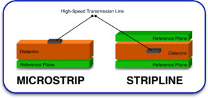
4. Controlled Impedance Traces
For high-speed designs, some traces need to have a controlled impedance, such as microstrip and stripline.
Microstrip: These traces are on the external layers of the PCB with a ground reference plane below.
Stripline: These traces are internal to the PCB, i.e., they are between two ground reference planes to reduce noise.
5. Follow Best Practices for Impedance Control
A single approach may not be sufficient for optimum impedance control. IPC standards or IPC-2141 provide recommended values for PCB trace impedance as a guideline for standardizing the PCB design.
6. Engage with Your PCB Assembler
Impedance-controlled PCB manufacturing and assembly require competitive process technology capabilities. The manufacturer must be engaged in stack-up construction, material choice, and fabrication process set-up and inspection.
Types of Impedance in PCB Design
In designing the board, the following types of PCB impedance must be considered:
1. Single-Ended Impedance
Single-ended impedance is the impedance of the single trace with respect to the ground that is carrying the signal. This is usually the case with regular signal transmission lines.
2. Differential Impedance
Differential impedance is associated with pairs of traces that carry complementary signals. Like USB, HDMI, and Ethernet, differential pairs require well-defined spacing and trace width for signal integrity.
3. Characteristic Impedance
A type of impedance unique to a particular trace on a PCB is called characteristic impedance. Characteristic impedance is determined by the dimension of the trace and the dielectric material surrounding it, which is important for high-speed designs.
4. Termination Impedance
Termination impedance is employed in signal sources and loads to eliminate impedance mismatch, which could lead to reflections. Series and parallel terminations allow proper impedance matching and control signal reflection.
Common Impedance Control Challenges and Solutions
1. Variation in PCB Fabrication Tolerances
Minor errors in PCB fabrication can affect impedance values. Solution: Contract an experienced PCB assembly services provider who guarantees tight fabrication tolerances.
2. Material Inconsistencies
Different PCB materials have different dielectric constants, which modify the impedance value. Solution: Use consistently high-quality dielectric materials from reputable suppliers.
3. High-Speed Signal Losses
The higher the frequency, the worse the signals become due to the skin effect and dielectric losses. Solution: Apply optimized tracing with low-loss material.
4.Cross Talk Between Traces
Closed-to-one trace paths have mutual coupling and can modify each other’s impedance. Solution: Provide adequate trace spacing and use ground planes for shielding.
At the end of the day, a proper control system is always necessary when implementing an advanced PCB design, especially in high-frequency and high-speed applications. This can greatly improve the integrity and dependability of signals and operations within the system. We at Blind Buried Circuits are experts at PCB design, fabrication, and assembly, and impedance-controlled PCB design and fabrication are one of our specialties. Feel free to contact us for custom PCBs with impedance matching or for any high-speed signal integrity issues. Let us help you ensure that your next PCB design meets industry standards. Contact us today!


