Making a proper PCB power supply layout is crucial for the satisfactory functioning of the printed circuit board, and it forms an essential building block for your electronic circuits. Inadequate power layout can cause unwanted noise, excessive voltage drops, overheating, or even total failure of the circuit. In this blog, we will discuss all practices that will enable you to design an efficient and dependable power supply circuit board.
It is always more helpful to focus on practical tips rather than theoretical concepts so that you can implement this tutorial in your next project. Whether it is your first time designing a PCB or you have some experience, this blog is aimed at helping you improve your layout to achieve better performance, longevity, and sustainability of the boards.
Importance of Power Supply Design
Every component mounted on your PCB depends on a reliable power supply. Detection of unexpected drops and spikes in a voltage range can result in malfunctioning components within the board design or, in the worst case, damaging them beyond repair. It comes as no surprise that power supply design standards should not be ignored. These components significantly improve layout practices, reducing inefficient execution results while maintaining optimal performance.
1. Plan Before You Route
- Start with a definite strategy.
- Consider how electricity moves around your board.
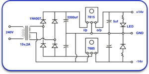
- Place power supply parts first: regulators, transformers, and inductors.
- Use trace-efficient routes for power lines.
- Make traces wide enough to carry current.
- Check your current values and verify trace width using online calculators.
2. Separate Power and Signal Paths
Combining power and signal lines may result in their interference with one another. Use different paths for them.
If your board is multi-layered, consider using different layers.
In general, keep high-power current paths further away from low-voltage signal lines.
This helps lower the amount of noise and crosstalk that may disrupt the normal functioning of your circuits.
3. Grounding: The Quiet Hero
The importance of a solid ground is equal to that of a power line. For maximum effectiveness, use a full ground plane. This gives your board a low-resistance return path and helps with heat dissipation.
If using a full ground plane is not an option, maintain short and wide ground paths. Each of your power components needs a clean, solid ground.
4. Decoupling Capacitors Should Be Included in Every Design
Decouple capacitors from each IC and place them near their corresponding power pins. This helps smooth spikes and lower noise.
Follow the values demonstrated in the component datasheet. A common range is 0.1µF to 10µF. Often, using both together is more effective.
5. Avoid Loops in Your Layout
Loops within your power or ground paths can produce noise problems because they act like antennas.
Make sure the return path follows the exact route taken by the outgoing trace. This creates a compact layout that minimizes electromagnetic interference (EMI).
Learn About : Best EMI and RF Sheilding Methods for Flex PCBs
6. Thermal Management Matters
Use thermal vias and copper pours to dissipate heat – power components can get hot.
Be sure to check the datasheet for your voltage regulators or switching components. Specific components require heat sinks or additional copper areas surrounding them.
7. Use Clear Labels and Test Points
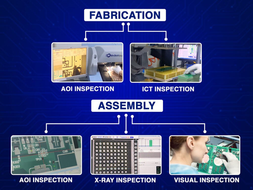
During PCB manufacturing and testing, make sure you or your technician have access to the voltages for easy checking. Also, make sure to add test points for the primary power rails.
Use silkscreen prints to indicate the voltage levels along with component names. This greatly streamlines the troubleshooting process later on.
8. Power Supply Area Utilization
When it comes to large circuits, clustering the power supply components helps tidy the design and keeps potentially noisy areas away from sensitive parts of the circuit.
For example, do not integrate the logic components with the motor driver or LED panel’s power components; instead, drive their outputs from separated low-powered sections.
9. Compliance with Guidelines for Quick PCB Fabrication
Like any other mass-produced product, there are general performance guidelines for fast PCB fabrication. Make sure that your power supply topology adheres to the following:
- Do not use 90-degree angles on signal traces; keep it at 45 degrees.
- Maintain adequate distance between high and low-voltage regions.
- Make sure that all the gaps are correct.
These steps improve the efficiency of many stages or assemblies in the PCB construction process, increasing their credibility and reducing the likelihood of board failure.
10. Selecting The Right Company for PCB Fabrication
Your design will be as competent as its fabricator. Choose a PCB fabricator who understands power supply topology requirements and is knowledgeable and equipped with MWDFM (Manufacturing with Design for Manufacturing).
Some fabricators assist in the design cycle, which will save you money spent on unreasonable pre-prepared alterations.
11. Collaborate WithCompetent Companies Offering PCB Assembly Services
The design is not the only factor affecting the board layout’s power. Strive to ensure that the firm provides assembly services so that the PCB works precisely according to your plans.
Proper component placement or incorrect soldering may cause issues with your power path. Remember, communication with your assembly team is essential.
12. Simulation Before Fabrication
Before you get to hardware testing, ensure that you use dedicated simulation software to verify the accuracy of your power layout. Free or paid, there are many tools available that check the current flow and can pinpoint problem areas.
Simulating your design is meant to fix problems early so that you avoid wasting valuable resources on a malfunctioning board.
13. Keep the Layout Simple
Avoid convoluted and complicated designs. In most cases, a clean, simple layout with short and clear paths works better.
Take a second look at your layout and try removing unnecessary vias, loops, or connections. A less complicated design is bound to be less likely to fail and easier to debug.
14. Learn from Existing Designs
Take the time to study other successful boards. Many open-nosed designs and development boards offer impressive performance, especially around the power layout.
Reviewing the layout of these designs can provide valuable insight into power routing, ground, and decoupling cap placement.
15. Think About Future Upgrades
When possible, leave the headroom while designing the power supply. For example, use components and traces rated at 1A if the circuit draws 500mA.
This reduces the need to redesign the entire board while increasing its reliability and offering flexibility for future changes.
Can make or break, your power supply layout defines your board. By adhering to the guidelines provided above, you can create boards that are dependable, efficient, and simpler to manufacture. These best practices are crucial if you are dealing with fast PCB manufacturing or tight schedules. Ensure that you have partnered with a reputable PCB manufacturing company and trustworthy PCB assembly services to realize your designs. Whether it is a hobby project or a commercial product, power layout planning is incredibly valuable. Use these principles to ensure a well-documented plan and check and recheck your work.
That is how to achieve a sturdy, stable, and successful power supply circuit board.

