If you’ve ever dealt with faulty electronics, you know how frustrating it can be. That’s why testing is one of the most essential steps in PCB manufacturing and assembly. It’s not just about building the board; it’s about making sure it works perfectly before it reaches the customer.
Design for Testability, or DFT, helps you do precisely that.
Whether you’re a product designer, an engineer, or working with a PCB manufacturing company, understanding DFT is key to building reliable circuit boards. Let’s explore what DFT means, why it matters, and how you can apply the proper steps during your following PCB manufacturing and assembly process.
What Is DFT in PCB Manufacturing?
Design for Testability (DFT) is the practice of designing your printed circuit board (PCB) so that it is easier to test after production.
Think of it this way:
If a board has issues, you want to find them early. But some designs make that really hard. With DFT, you build your layout to allow for easier access, smarter checks, and faster detection of problems before the product leaves the factory. This makes DFT important for every PCB manufacturing company that wants to reduce failures and rework.
Why DFT Matters?
Here’s a simple truth:
The earlier you catch a mistake, the cheaper it is to fix. Without proper PCB testing, faulty boards can go unnoticed until they’re inside a product. That means expensive repairs, replacements, or even recalls. With DFT in place, testing becomes part of the design, not an afterthought. And this isn’t just about saving money. It also protects your brand, your customers, and your reputation.
PCB Testing Methods You Should Know
Before we jump into DFT guidelines, it helps to know how PCBs are tested. Here are the most common PCB testing methods:
1. In-Circuit Testing (ICT)
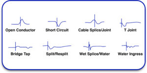
ICT checks each component on the board. It uses a bed-of-nails fixture to connect test points on the PCB. This method is very accurate and fast but needs test access built into the board.
2. Flying Probe Testing
Flying probes use tiny needles that move around the board to check for shorts, opens, and component values. It’s slower than ICT but great for low-volume runs and prototypes.
3. Functional Testing
This test powers up the board and checks if it performs its job. It simulates real-world use to make sure everything works as expected.
4. Boundary Scan Testing
This method checks digital parts of the board without physical test probes. It’s helpful when access to test points is limited.
All of these methods depend on how the board is designed. That’s where good DFT comes in, making testing possible and effective.
Learn About: The Critical Methods in PCB Testing and Inspection
Key DFT Guidelines for Better PCB Testing
Now, let’s look at how you can design your board for better PCB testing and inspection.
1. Add Test Points Early
Make sure every signal and power net can be reached. Add test points for all critical signals. You’ll need those access points if you plan to use ICT or flying probe tests.
Mark these clearly on your layout, and make sure they don’t interfere with components or connectors.
2. Keep Test Pads Uniform and Spaced
Try to make all your test pads the same size. Keep enough space between them so that test needles or probes can land without error.
Too close, and the test might fail. Too far apart, and you might run out of room.
3. Group Test Points When Possible
If possible, group related test points together. This reduces test time and helps organize your board layout.
This also helps your PCB manufacturing company build fixtures more easily if needed.
4. Design with Test Fixtures in Mind
Not all boards will use the same PCB testing methods. Some need fixtures. Others rely on probes.
Talk with your PCB manufacturing and assembly partner early. Ask them how they plan to test the board and adjust your layout to match.
5. Allow for Power Isolation and Measurement
It’s smart to include jumpers or resistors that allow you to isolate and measure current on power rails. This makes power PCB board testing much easier.
For example, during a short-circuit test, you can remove a jumper and measure current without damaging the board.
6. Use Accessible Component Values
Where possible, don’t bury key components under shields or behind connectors. Make them easy to reach with a probe.
This allows your PCB manufacturing company to validate component values during the test step.
7. Label Everything Clearly
Use silkscreen labels to identify test points and essential components. This helps both automated and manual testers know what they’re checking.
It’s a simple step that can save hours of confusion during PCB testing.
PCB Testing Challenges Without DFT
Skipping DFT can lead to several issues. Here are some real-world problems caused by poor test planning:
- No access to signals means longer debugging time.
- Fixtures are expensive or impossible to build.
- Failures go undetected until final product testing.
- Technicians can’t verify components during PCB board testing.
- Test probes damage nearby parts because of tight spacing.
If you’re working with a PCB manufacturing company, not following DFT guidelines can cost both sides time and money.
When Should You Start Thinking About DFT?
Right from the start:
DFT should be part of your layout planning —not something you fix later. The sooner you think about PCB testing methods, the better your final board will be.
-
During the schematic phase, plan which signals and power lines need access.
-
During layout, place test pads and consider probe spacing.
Work closely with your PCB manufacturing and assembly team. Ask them for input and feedback. They’ve seen what works and what causes delays.
Tips for Working with Your Manufacturing Partner
Your board design doesn’t exist in a vacuum. You’re working with a PCB manufacturing company to bring it to life.
Here’s how you can make that partnership smoother:
- Ask about their preferred testing methods. Don’t guess, find out what works in their process.
- Share your test strategy early. If you know what’s important to test, include it in your design notes.
- Use standard pad sizes and footprints. This helps them build fixtures or use flying probes more easily.
- Review test access before finalizing the design. Catch issues before they cost money.
Final Thoughts
Good testing makes good products. But good testing starts with smart design.
By following these DFT guidelines, you’ll make life easier for your testing team, reduce the risk of faulty boards, and deliver a better end product. Whether you’re building one board or a thousand, planning for PCB board testing from day one helps you stay on time and budget. So, the next time you start a project, remember that designing for a Test is not extra work; it’s the smart way to build. Would you like this turned into a downloadable checklist or print-ready guide next?


