The miniaturization of electronic devices makes PCB thermal management more challenging than ever. Too much heat can lead to performance deterioration, component failure, and system malfunctions. Comprehensive thermal solutions for PCBs must be integrated during and following the PCB manufacturing assembly process for optimal efficacy. In this blog, we will delve into 12 different proven techniques for optimizing your PCB board assembly manufacturing in terms of heat management and reliability, thus optimizing your yield and quality.
Basics of PCB Heating
The sources of heating in a PCB are usually active components like processors, power transistors, and voltage regulators. If left unmanaged, excess heat will invariably cause thermal stress, component degradation, or circuit failure.
Some common causes of PCB heating are:
– High current flow through traces
– Poor ventilation due to dense component placement
– Material limitations resulting in insufficient heat dissipation
– Absences of thermal vias or heat sinks
In order to mitigate these risks, manufacturers resort to sophisticated techniques of PCB thermal management.
12 Approaches for Proper PCB Thermal Management
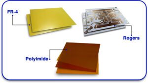
1. Employ PCB Materials with a Very Good Thermal Conductivity
The type of substrate selected will largely determine how well heat can be dissipated. The commonly used FR-4 PCB materials have poor thermal conductivity, while other materials, such as ceramics, high-power metal cores, and laminates, have high-performance heating materials.
Best Recommended Materials for PCB Thermal Management:
- MCPCB (Metal core PCBs): Don’t forget these when designing for LED and high-power applications.
- Rogers and Polyimide laminates: These work well with high-frequency and aerospace applications.
- Aluminum-backed PCBs: These are ubiquitous with power electronics and automobile applications.
2. Enhance Thermal Functionality by Optimizing the PCB Layer Stack-Up
Properly designed PCB stack-ups provide better heat distribution across the board. Internal copper layers help eliminate hotspots, thus improving heat dissipation.
Recommended Practices for PCB Stack-Up:
- Increase the layer thickness of copper to achieve better conductivity.
- Position the power and ground planes close to the heat-producing parts.
- Use internal thermal planes in multi-layer PCBs to efficiently spread the heat throughout the panel.
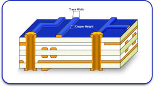
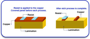
3. Improve Heat Dissipation by Increasing Copper Thickness
While copper traces conduct electricity, they can also dissipate heat. Thicker copper layers can be used, and PCB board assembly manufacturing can be done at a different level, resulting in better heat dissipation.
Copper Thickness Recommendations:
- 1oz copper (35 µm) – Commonly accepted value for most PCBs.
- Heavy copper ( 4+ ounces) works best for any high-current tasks.
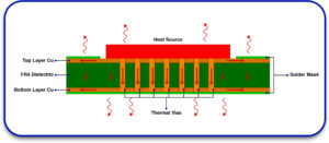
 4. Adding Thermal Vias for Heat Movement
Thermal vias are tiny plated holes that allow the interconnection of heat-producing components to other inner or bottom layers, allowing heat to be lost.
Types of Thermal Vias:
- Through-hole thermal vias: Multi-layer heat spreading is known as the best.
- Blind/buried thermal vias: Used in HDI PCBs for selective heat transfer.
- Filled thermal vias: Conducting paste is used to improve thermal conductivity.
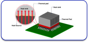
5. Adhere to Thermal Pads and Heat Sinks
Heat sinks are placed on power transistors and CPU devices to radiate heat. This allows for more easily removing excess thermal power. The use of thermal pads improves contact with the component, making the transfer of heat more efficient.
Choosing the Proper Heat Sink:
- Passive heat sinks: Cooling is done by natural convection.
- Active heat sinks: Fans with forced air cooling are present.
- Bonded fin heat sinks: For use in high-power applications.
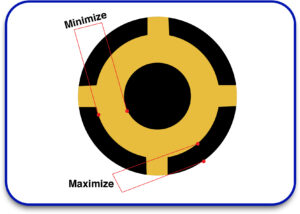
6. Use Thermal Relief Pads to aid the stability of soldering
While large copper areas aid in heat removal, they may draw too much heat away from the solder joints, resulting in poor soldering. Thermal relief pads help balance heat dissipation and solderability.
Thermal Relief Pad Best Practices:
- Use cross-hatched copper connections for better heat removal. Dial in the spoke width to optimize heat transfer.
- Pay close attention to the routing of power traces and current carrying vias to ensure the placement is correct.
7. Improving Component Layouts for the Best Possible Results
Particular components on a PCB contribute significantly to its heating. For example, if you place heat-emitting components in corners or regions with good airflow, they will cool off more easily.
Guidelines on Component Layout Design:
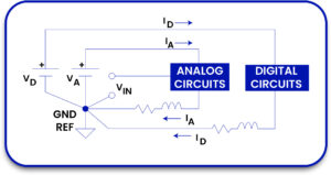
- Separate power components with sensitive analog circuits.
- Put high-power dissipation components close to thermal vias or heatsinks.
- Ensure components are not packed too tightly together because they may retain heat.
8. Applying Thermal Barriers and Other Insulating Methods
Some barriers stop heat from reaching sensitive components. Materials like Kapton tape or layers of thermal insulation may be added to shield critical areas.
Applications of Thermal Insulation:
- Covering low-power integrated circuits from high-power sections.
- Blocking sensors from external heating.
- Minimizing the thermal impact on the more fragile SMD components.
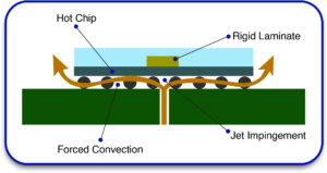
9. Using Active Cooling Methods
Active cooling methods, such as liquid cooling and fans of any type, are obligatory for the construction/assembly of high-powered PCBs.
Active Cooling Methods:
- Forced air cooling, such as with fans or blowers – They blow heat away from the board.
- Liquid cooling, such as with cold plates or heat pipes, achieves an effective heat transfer rate, specifically for industrial PCBs.
- Peltiers, or thermoelectric modules, are coolers. They are very effective in areas with extreme temperatures.
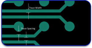
10. Reduce the Width and Gap of The Trace
Narrower traces lead to increased resistance and heat buildup, while wider ones dissipate heat. Effective PCB trace design with optimal widths and spacing minimizes resistance and localized heating issues.
Trace Width and Gap Recommendations:
- High-current paths should always use wider traces to reduce resistance and heat production.
- Spacing between adjacent traces must be sufficient to avoid thermal crosstalk.
- Sticking to IPC-2221 standards with regard to trace width and their current carrying capacity is a good practice.
11. Reduce Locally Stored Heat Using Heat Spreaders
The inclusion of thermal mass can better distribute the heat generated by a PCB, reducing the risk of overheating. This is accomplished by strategically increasing copper areas or using embedded heat spreaders.
Helpful Tips To Increase Thermal Mass:
- Enlarge the area of ground and power planes for heat distribution.
- Place copper pours around the heat-generating components.
- Use embedded heat pipes for extreme thermal applications.
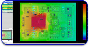
12. Perform Accurate Thermal Simulations On PCB’s
Advanced simulation software like ANSYS, SolidWorks, and Altium Designer is helpful in predicting thermal behavior. Engineers use these programs to spot hot spots and optimize cooling approaches before the system goes into production.
Advantages of Thermal Simulation:
- Gives estimates on thermal dispersion across the PCB.
- Aids in component arrangement with the aim of enhancing cooling.
- Helps to prevent overheating failures in the last production stage.
To learn more, see PCB Thermal Profiling in PCB Assembly
Properly managing PCB thermal systems is vital in achieving long-term reliability and performance. These 12 actionable methods can help engineers address PCB heating challenges and enhance overall efficiency in PCB board assembly manufacturing. At Blind Buried Circuits, we pride ourselves on manufacturing assembly PCBs with superior thermal management solutions. Whether you are looking to design a custom PCB or need assistance with thermal management, we have you covered.
Contact us so that we can assist you in optimizing your PCB designs for enhanced heat dissipation and extended durability.


