A smooth process of PCB manufacturing and assembly starts with proper design planning. Errors that occur in the early design steps can lead to problems during the PCB board assembly manufacturing phase, which can potentially be very expensive, both in terms of time, money, and effort. In this article, you will get a glimpse of the top 6 reasons that lead to assembly failures and how to avoid them. This will help you increase product quality, reduce costs, and carry out PCB manufacturing and assembly in an effective and time-conscious manner.
1. Missing Information or Misalignment in Design Files
Make sure that the design documentation is complete and precise for any PCB assembly. Poor or incomplete design files can cause assembly inaccuracies such as wrong footprints, unplaced solder masks, or even misplaced components, which can lead to dire manufacturing consequences.
Key File Issues To Be Concerned About:
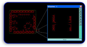
Gerber File Problems:
- Layers that are pasted improperly or are absent can impede the signal from passing through.
- Mistakes with drill holes, like incorrect positions or sizes, can affect the placement of parts.
- Errors in file format may prompt miscommunication or loss of data between the designer and the manufacturer.
Centroid File Mistakes:
- Improperly placed component coordinates will mount these components in the wrong positions.
- Not properly orienting components may lead to final assembly issues.
Solder Stencil File Troubles:
- Issues often include the solder paste not being applied correctly. This misapplication is due to misaligned apertures or the incorrect aperture size.
- Solder bridges can also happen when the aperture overlaps.
What Steps Should Be Taken to Avoid These Issues:
In order to avoid errors in PCB manufacturing and assembly:
- Thorough checks of the drawing rules in DRC should be done before the Gerber files are created.
- The positions of the components and the layout of the centroid file should be of the same unit.
- Align stencil apertures with the appropriate stencil thickness.
- Effective examination of the design files and quality checks can help prevent expensive errors and make the assembly more efficient.
2. Errors regarding the Bill of Materials or BOM
The components needed in assembling the PCB are included in the BOM. Failure to create this document accurately can result in assembly problems and delays in sourcing.
BOM Issues that Are Common:
- Wrong Part Number: Due to the wrong part number, the components can be sourced incorrectly.
- Components Missing: Not including components on the BOM will result in half-finished assemblies.
- Having Multiple Submissions: Putting the same information more than once will confuse people who order parts.
- Out-of-date Parts: Dealing with old parts that are no longer available will make it difficult to source them.
Solutions:
- Check the part numbers against the appropriate datasheets for accuracy.
- Use software that validates BOM to catch duplicate entries and errors.
- The BOM should be checked and improved to include new components that replace the ones that cannot be found.
- Always check the vendors to have the right information to buy from them within the time frame needed.
- A well-organized and precise BOM provides better productivity and improves accuracy in your PCB board assembly manufacturing system.

3. Errors in the Placement of Components
The placement of components on the PCB is vital for the PCB manufacturing and assembly to function properly. If not done correctly, it will result in component misalignment, soldering difficulties, and non-functionality.
Placement Errors that are Commonly Seen:
- Misplacing Components: Misplacing components results in “tombstoning,” where certain parts stand on the PCB instead of lying down during soldering.
- Improper Positioning: Components such as diodes and capacitors with reverse polarity will not allow the circuit to work.
- Different Heights: Taller components can obscure smaller ones during wave soldering.
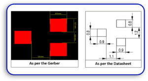
- Improper Footprints: If the footprint of the components is larger than their actual physical size, they are useless.
The Correct Way to Do It:
- Indeed, the correct way is to examine the component datasheets to confirm the orientation.
- For solder pads, always keep the mask openings for pads with a ratio of 1:1.
- While wave soldering, always put the short parts behind the tall ones.
- The component’s footprints should be checked to ensure that they are the correct sizes.
- These efforts can spare a business from expensive rework and increase assembly efficiency.
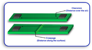
4. Lack of Sufficient Clearance Allowance
For effective assembly of the device, there must be space between components and openings of copper features. Lack of sufficient space can result in electrical shorts, damage to mechanical components, and difficulties in testing.
Solder Clearances Which Are Problematic:
- Clearance between Component and Component: Narrow spacing between components can hinder soldering unwanted joints.
- Features To-Copper Components: Traces that are too close to parts may result in shorts.
- Component-to-Board Edge: Parts placed near the board edges are more prone to damage.
- Solder Mask Incursion: The pad clearance beneath the solder mask is too close, which nullifies the board’s reliability.
Clearance Checklist:
- A minimal spacing of 6 mil clearance for tiny components and 39 mil for sensitive devices such as BGAs should be observed.
- Components must be at least 50-75 miles away from the board edges.
- To prevent solder mask incursion, 1.6 mils should be incorporated between the edges of the pads used for the solder mask.
- The above stated spacing rules will help minimize mistakes being made during PCB assembling and manufacturing processes.
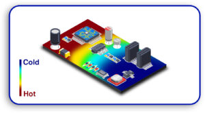
5. Inadequate Heat Management
Proper thermal management guarantees that all devices will function properly without surpassing their maximum rated temperatures. This applies when joints are susceptible to weakening due to extreme heat or soldering mechanical failure.
Thermal Related Problems:
- Lack of Heat Dissipation: If there are no sufficient ways of dissipating heat, components can overheat.
- Thermal Relief Inadequacy: Some of the Through-hole components may fail to solder without these supports.
- Obstructed Airflow Channels: The placement of these components can cause absorption of the heat that is meant to be expelled.
Suggested Solutions:
- Incorporate heatsinks, thermal vias, and fans as a way of dealing with heat.
- Provide four evenly distributed thermal spokes for through-hole components.
- Relocate components to improve airflow.
Staying ahead by managing the dissipation of heat will improve the performance of the board and boost its reliability.
6. Inadequate Coverage of PCB Testing as an Issue
Effective testing before production can easily mitigate product defects. Testing is crucial prior to production as it helps uncover any potential hitches, which are dealt with with limited tests.
Some common testing problems include:
- Not Enough Test Points: Some measurements may go untested, resulting in difficulties with detecting errors.
- Incorrectly Placed Test Points: Components that may be too close to the test points can affect placement.
Use of Test Points
- The correct usage of test pads, vias, and through-holes without solder resistances allows for easy access.
- Spacing between components and test points is crucial.
- Design and fabricate test fixtures that will enhance the contact and alignment precision of the tested object.
- Thorough testing guarantees high-quality assembly devoid of defects.
By correcting the design errors noted, the process of producing and assembling PCBs will be smoother and more efficient. By providing correct design data, managing blank cut sheets, improving the configuration of the components, providing adequate clearance, controlling the escape of heat, and improving testing, you will be able to facilitate adherence to schedule and improve the product.
We encourage you to contact our specialists at Blind Buried Circuits if you require assistance with PCB manufacturing and assembly. Our goal is to help you improve your assembly process and the quality of the product.


