Printed Circuit Boards, or PCBs, are the backbone of modern electronic devices, powering everything from smartphones to medical equipment. Ensuring PCBs are safe and work as they should is critical, and one key factor is proper line spacing. This article explains why line spacing is so important, how it affects safety, and what steps you can take to get it right. We will discuss concepts such as clearance creepage and emphasize why it is critical to work with a reputable PCB board manufacturer.
Why Proper Line Spacing is Important
The line spacing appears to be one of the little things in the design, but it plays a huge role in how a PCB will function. Here’s why it matters:
- Prevents Electrical Short Circuits: When the lines are sufficiently spaced apart, the likelihood of short circuits through accidental arcing or debris buildup is minimized.
- Improves Electrical Insulation: Proper spacing makes sure that there is no unwanted flow of electricity between components.
- Reduces Electromagnetic Interference (EMI): Good line spacing helps in reducing EMI, which could interfere with other electronic parts.
- Meets Industry Standards: Organizations like IPC specify certain spacing rules to make PCBs safe and reliable.
- Increases Longevity: Proper spacing decreases the stress on the board, making it work for a long time, even under demanding conditions.
Understanding Clearance and Creepage
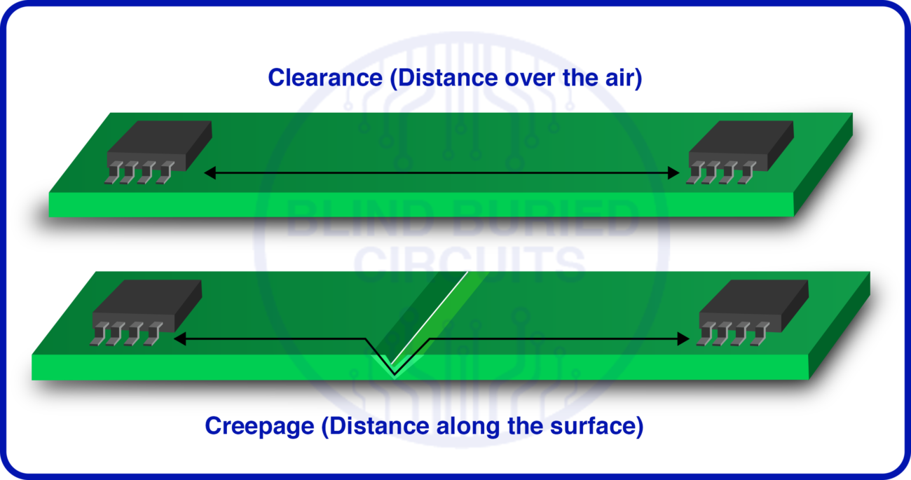
The most important aspect of PCB design is clearance creepage. These terms define the minimum space required to keep electricity flowing where it should:
- Clearance: This is the shortest distance between two conductive parts in the air. It’s critical for avoiding electrical arcs.
- Creepage: This is the shortest path electricity can take along the surface of an insulating material. Factors like dust, humidity, and temperature can affect creepage.
By designing PCBs with proper clearance and creepage, you can prevent failures, especially in high-voltage or high-frequency circuits. Ignoring these details can lead to electrical tracking, which can damage the board or even cause a fire.
Factors That Influence Line Spacing
Different PCBs have different requirements for line spacing, depending on their intended use. Here are some factors to consider:
- Voltage Levels: Higher voltages require larger spacing to ensure safety.
- Environmental Conditions: Moisture, elevation, and contaminants may contribute to the failure of insulation.
- Material Properties: PCB substrate material has a bearing on the amount of clearance and creepage required.
- Design Complexity: Designs with closely packed components require detailed considerations to ensure adequate space between lines.
- Regulatory Compliance: Compliance with standards such as IPC-2221 will assure you that your design is cleared for use by most industries.
How to Have Proper Line Spacing
To optimize your line spacing for your PCB, follow these instructions:
- Follow Industry Standards
Start from the guidelines laid down by the standards like IPC-2221. These define minimum clearance and creepage distances based on conditions such as voltage. Following industry standards ensures your design will clear safety inspections.
- Team up with a Reliable PCB Board Manufacturer
Work with an experienced PCB board manufacturer such as Blind Buried Circuits. Manufacturers know their line spacing is critical and prevent costly errors in their design.
- Opt for Quality Material
Use high-dielectric-strength materials such as FR4 or Rogers to reduce the chance of insulation breakdown. Your manufacturer can advise you on the best material to use based on your specific application.
- Use the Best Design Software
Modern PCB design software can assist in calculating the clearance and creepage spacing needed. However, all such calculations must be checked by an expert for accuracy.
- Test Thoroughly
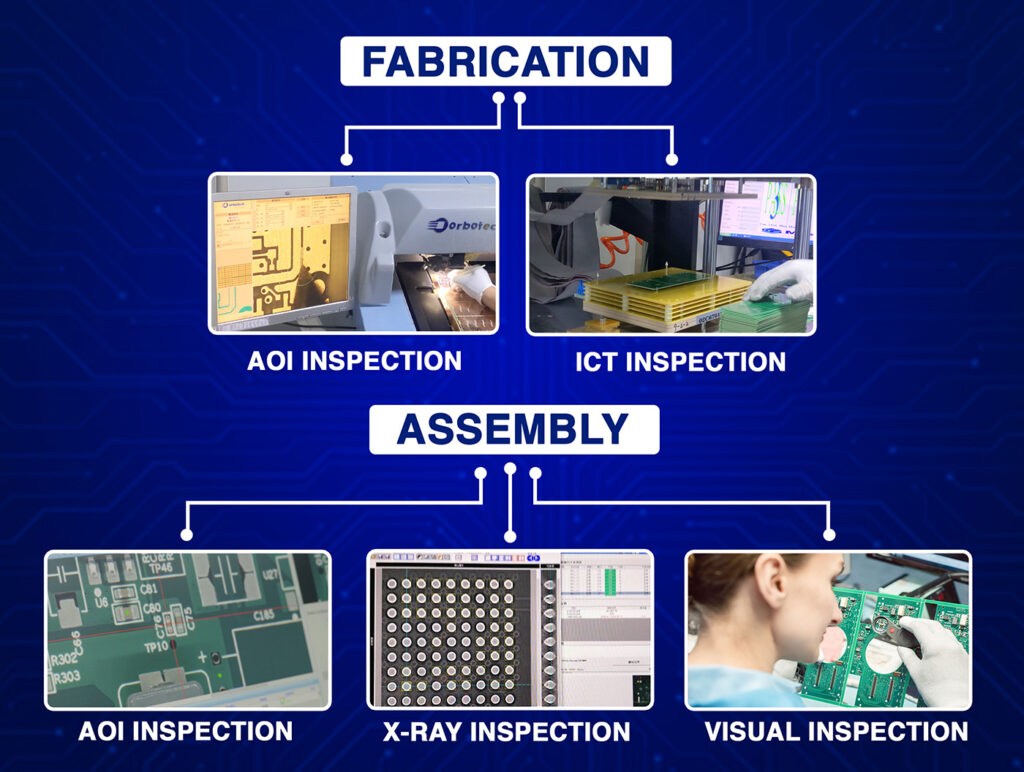
Testing is essential to catch problems before production. For instance, high-potential (HiPot) testing can confirm whether the clearance and creepage distances comply with safety requirements.
- Consider Future Upgrade
Sufficient provision should be made for potential design requirements in the future. It can help you save time and resources during later versions.
Bonus Tips
- Check PCB Layouts Carefully: Errors made in the design stage can result in expensive rework. Verify all spacing calculations.
- Pay Attention to Environmental Conditions: If your PCB is to be used in hostile environments, select materials and designs that can handle these conditions.
- Record Your Design: Track all design decisions to make it easier to debug and upgrade.
Proper line spacing is critical to the safety and reliability of PCBs. Understanding the importance of clearance creepage and best practices and working with a trusted PCB board manufacturer can create designs that will perform well under all conditions. At Blind Buried Circuits, we’re here to help you every step of the way, from design to production.

