Building a prototype printed circuit board (PCB) from scratch is a rewarding process that brings your electronic design ideas to life. Whether you’re a student, hobbyist, or professional engineer, mastering the PCB prototyping process will significantly enhance your hardware development skills.
This blog outlines each phase of PCB prototyping from initial planning to final testing, so you can confidently bring your concept into the real world.
1. Define Your Project Requirements
Before opening any design software, it’s essential to outline clear objectives and technical constraints.
Understand Your Functional Goals
- What is the core purpose of the PCB?
- Will it control a motor, sense the environment, or process data?
Set Size and Form Factor Limits
- What dimensions must your PCB fit within?
- Are there mounting holes, casing, or connectors that dictate the shape?
Determine Electrical Specifications
- What are the voltage and current requirements?
- Will it operate from batteries, USB, or an external power supply?
Identify Key Components
- Decide on microcontrollers, sensors, switches, connectors, etc.
- Check availability and datasheets before finalizing selections.
Having this foundation ensures that your design phase is aligned with both practical and functional goals.
2. Create a Schematic Diagram
The schematic is the logical representation of your circuit and is a critical step in your design process.
Choose EDA Software
- Popular tools include KiCad (open source), Autodesk Eagle, Altium Designer, and EasyEDA.
- Choose one that suits your budget and experience level.
Add and Configure Components
- Insert symbols for resistors, capacitors, ICs, etc.
- Configure attributes like values and footprints.
Draw Electrical Connections
- Connect pins using “nets” that indicate signal paths.
- Use labels for shared connections to keep things clean.
Validate Your Schematic
- Double-check pin connections, polarities, and power supply routes.
- Use ERC (Electrical Rule Check) tools to catch design errors early.
Learn About: Why is a Schematic Diagram Important for PCB Manufacturing?
3. Design the PCB Layout
The PCB layout is a physical representation of your schematic and affects performance and manufacturability.
Optimize Component Placement
- Group components logically by function (e.g., power section, microcontroller, outputs)
- Minimize signal path lengths and avoid placing sensitive analog parts near noisy digital signals.
Route Traces Effectively
- Use wide traces for high-current paths.
- Keep differential pairs matched in length.
- Use 45° angles rather than 90° for signal integrity.
Use Ground and Power Planes
- Add solid copper planes to reduce EMI and improve performance.
- Decouple power supplies with capacitors near ICs.
Apply Design Rules
- Run a DRC (Design Rule Check) to ensure clearances, trace widths, and via sizes meet manufacturing specs.
4. Generate Manufacturing Files
With the layout complete, it’s time to prepare files for production.
Export Gerber Files
- Include layers such as top/bottom copper, solder mask, silkscreen, and drill data.
- Use the correct file naming conventions required by manufacturers.
Create a Drill File
- Provides data for hole sizes and locations for vias and through-hole components.
Prepare the Bill of Materials (BOM)
- List all components, part numbers, values, and quantities.
- Include manufacturer part numbers to reduce ambiguity.
Include a Pick-and-Place File (Optional)
- For automated assembly, this file gives component locations and orientations.
5. Choose a PCB Manufacturer
Not all manufacturers are created equal. Select one based on your specific needs.
Evaluate Capabilities
- Can they support multi-layer boards, fine pitches, or specialized materials?
Compare Pricing and Turnaround Times
- Some offer low-cost prototypes with slower shipping; others specialize in rapid prototyping.
Check Reviews and Support
- Ensure the manufacturer has reliable customer service, especially if you’re new to PCB fabrication.
Ask About Quality Control
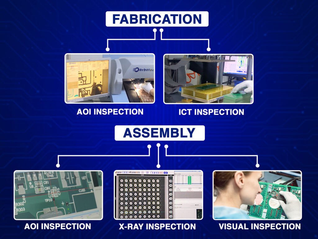
- Look for AOI (Automated Optical Inspection), impedance control, and electrical testing services.
6. Fabrication and Assembly
Your design now moves from digital to physical.
PCB Fabrication Process
- Laminating: Layers of copper are bonded to insulating material.
- Etching: Excess copper is removed to form traces.
- Drilling: Holes are made for component leads and vias.
- Solder Mask & Silkscreen: Protects copper and adds labels.
PCB Assembly Process
- Solder Paste Application: Applied to pads for SMD components.
- Pick and Place: Machines place components on the board.
- Reflow or Wave Soldering: Components are soldered to the board.
- Manual Assembly: Used for low-volume or through-hole components.
Learn About: The Role of Flying Probe Testing in PCB Assembly
7. Testing and Validation
This is the step where theory meets reality.
Visual Inspection
- Look for solder bridges, misaligned components, and missing parts.
Continuity and Electrical Testing
- Use a multimeter or continuity tester to ensure correct connections and no shorts.
Functional Testing
- Power the board and test in its real-world application.
- Check communication protocols, sensor readings, and output signals.
Debugging Techniques
- Use an oscilloscope or logic analyzer for signal-level issues.
- Compare expected vs. actual behaviors based on the schematic.
8. Iterate, Refine, and Improve
No prototype is perfect on the first try. Iterate for better performance and manufacturability.
Update Your Design
- Incorporate feedback from testing.
- Replace parts with better or more available alternatives.
Revise the BOM
- Use standard or preferred components to reduce cost and lead times.
Optimize Layout for Production
- Improve trace routing, component spacing, and mechanical stability.
Document Everything
- Maintain version control of design files, test results, and revisions.
9. Prepare for Mass Production (Optional)
Once your prototype is validated, consider scaling to larger production.
Design for Manufacturability (DFM)
- Ensure your design meets manufacturing constraints for high-volume production.
Source Reliable Suppliers
- Build relationships with trusted component and assembly partners.
Plan for Testing at Scale
- Develop test jigs and procedures for fast, consistent verification.
Conclusion
Building a PCB prototype from scratch is a structured yet creative process that blends electronics knowledge, design tools, and manufacturing coordination. By understanding and refining each phase, from project definition to final testing, you’ll gain the skills needed to bring sophisticated electronic ideas to life.
Always remember: prototyping is not just a technical exercise, but a cycle of learning, iteration, and improvement. The more detail and care you invest, the more successful your final product will be.


