Are you struggling with routing high-density PCBs?
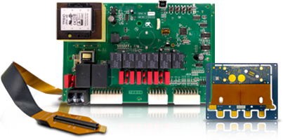
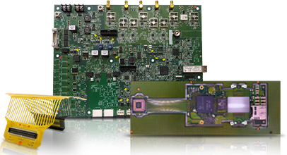
As electronics get smaller and more powerful, think smartphones, wearables, and compact medical devices, engineers are turning to High-Density Interconnect (HDI) PCB designs. HDI allows more functionality in a smaller area, but it also brings new routing challenges that traditional PCBs don’t have. In this article, we’ll explore the most common HDI PCB routing problems and show you how to solve them step-by-step. Whether you’re new to HDI or looking to improve your existing designs, this guide will help you make smarter design decisions and reduce errors before they become expensive problems.
What is an HDI PCB?
HDI in Simple Terms
A High-Density Interconnect (HDI) PCB is a circuit board with more connections per unit area than standard PCBs. It uses:
- Smaller vias (like microvias)
- Finer trace widths
- Higher component density
This allows you to fit more electronics into less space, which is essential for modern, compact devices.
Common HDI PCB Routing Challenges and How to Solve Them
1. High Component Density and Routing Congestion
The Problem
HDI boards pack many tiny components into tight spaces. This makes it difficult to route all the connections without creating a tangled mess or violating spacing rules.
How to Fix It
Group Related Components
- Place components that work together (like decoupling caps and ICs) near each other.
- This shortens trace lengths and makes routing cleaner.
Place Critical Components First
- Put key parts, like microcontrollers, memory, and connectors, early in the layout.
- Route their signals first before handling less critical paths.
Use Smaller Packages
- Consider Ball Grid Arrays (BGAs) or small-outline SMD parts to save room.
Use Design Rule Checks (DRC)
- Your PCB design software can automatically check for spacing issues.
- Run DRC early and often to avoid expensive errors later.
2. Signal Integrity and Impedance Control
The Problem
When traces are packed closely and signals move fast (especially above 100MHz), signal integrity becomes a big issue. Crosstalk, reflection, and timing problems can affect performance.
How to Fix It
Use Controlled Impedance Routing
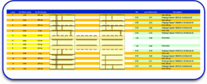
- Match trace widths and spacing based on your board’s stack-up.
- This prevents reflections and signal distortion.
Route Differential Pairs Properly
- Keep the pairs close together and of equal length.
- Perfect for USB, HDMI, or high-speed serial interfaces.
Add Guard Traces
- Place grounded traces next to sensitive signals to reduce interference.
Match Trace Lengths
- Necessary for signals that must arrive at the same time (like clocks or data buses).
Learn About: Crosstalk in High-Speed PCB Design: Causes and Solutions
3. Thermal Management and Heat Dissipation
The Problem
More components = more heat. In HDI boards, there’s often little room for heat to escape. Poor thermal design can lead to overheating and component failure.
How to Fix It
Add Thermal Vias
- Use vias to transfer heat from hot components to the inner or bottom layers.
- Works like tiny “chimneys” for heat.
Use Heat Sinks or Heat Spreaders
- Place them on power-hungry chips like voltage regulators or processors.
Make Traces Wider for Power Paths
- Wider traces reduce resistance and heat buildup.
Choose the Right Material
- Some PCB materials (like FR-4 alternatives) offer better heat conductivity.
4. Manufacturing Constraints
The Problem
HDI boards need exact manufacturing. Tight tolerances, fine features, and special via structures can push some fabricators beyond their limits.
How to Fix It
Communicate Early with Manufacturers
- Talk to your PCB house during the design phase, not after.
- Ask about capabilities, limits, and preferred design rules.
Follow DFM Guidelines
- DFM = Design for Manufacturability.
- Stick to your manufacturer’s recommended spacing, via sizes, and stack-up.
Use Standard Processes Where Possible
- Avoid exotic via structures or rare materials unless necessary.
5. Via Management
The Problem
HDI boards use lots of vias, especially microvias, to connect tight layers. If not managed well, vias can block routing paths, increase cost, and cause reliability issues.
How to Fix It
Use Microvias Wisely
- Microvias connect adjacent layers without taking up much space.
- They’re great for tight areas but more expensive, so use them where needed.
Consider Via-in-Pad Techniques
- Save space by putting vias directly in BGA pads.
- Ideal for tight BGA layouts, but they must be filled and capped correctly.
Distribute Vias Strategically
- Don’t cluster all your vias in one corner.
- Spread them out to reduce stress on the PCB and improve routing flow.
6. Power Distribution and Noise Reduction
The Problem
As power needs increase, voltage drops and electrical noise can disrupt performance. Dense layouts can worsen this problem by creating longer power paths and ground loops.
How to Fix It
Use Dedicated Power and Ground Planes
- Allocate full layers for power and ground to improve stability and reduce noise.
Add Decoupling Capacitors
- Place them as close as possible to IC power pins.
- They smooth out the voltage and filter the noise.
Use Stitching Vias
- Connect ground planes across multiple layers using stitching vias.
- This helps create a low-impedance ground return and reduces EMI.
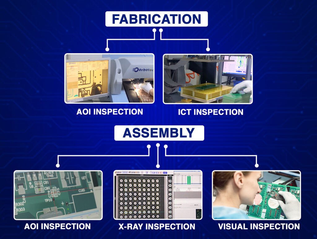
7. Testing and Accessibility
The Problem
HDI boards are rigid to probe and test manually. Small traces and hidden pads make inspection difficult.
How to Fix It
Add Test Points
- Even if they’re tiny, test points let you validate signals during debugging.
Use Bed-of-Nails Fixtures for Volume Testing
- Automated testers can contact key nodes through spring-loaded pins.
Plan for Accessibility
- If possible, don’t hide critical test traces or pads under BGAs.
Best Practices for Successful HDI PCB Routing
Now that you’ve seen the main challenges, let’s summarise the top habits that lead to successful HDI routing.
Collaborate from the Start
- Work with PCB manufacturers, assemblers, and even component suppliers early.
- Avoid surprises at the production stage.
Use the Right Design Tools
- Choose CAD software that supports HDI features like blind vias and impedance simulation.
Simulate Before You Build
- Use simulation tools to test thermal behaviour and signal integrity before production.
Prototype and Iterate
- Build prototypes to test in the real world.
- Validate everything before moving to high-volume manufacturing.
Final Thoughts
Designing HDI PCBs is more complex than working with standard boards, but the payoff is enormous. You get smaller, lighter, and more powerful devices. The key is understanding the unique challenges that come with high-density routing and knowing how to address them early.
To recap:
- Plan component placement carefully
- Manage vias smartly
- Keep signal integrity and power stability in check.
- Work closely with your manufacturer.
- Use advanced tools and simulations.
By following these principles and solutions, you can confidently tackle HDI routing challenges and create reliable, production-ready boards.

