Designing high-speed PCBs requires a deep understanding of electrical interference, especially crosstalk. If not properly managed, crosstalk can degrade signal quality, cause data errors, and impact overall PCB performance. As a pcb manufacturer or an engineer working on pcb board assembly manufacturing, knowing how to minimize crosstalk is essential.
This blog will discuss what crosstalk is, why it happens, and how you can reduce it in high-speed PCB designs.
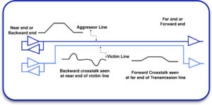
What is Crosstalk in PCB Design?
Crosstalk occurs when signals from one PCB trace interfere with signals in nearby traces. This unwanted interference can cause performance issues in high-speed applications such as networking devices, communication systems, and computing hardware.
There are two main types of crosstalk:
- Near-End Crosstalk (NEXT): This happens when a signal is induced at the transmitting end of the affected trace.
- Far-End Crosstalk (FEXT): This occurs when the interference is detected at the far end of the affected trace.
Both types of crosstalk can disrupt signal integrity, leading to data corruption and increased error rates.
What Causes Crosstalk in High-Speed PCBs?
Crosstalk in high-speed PCB design happens due to several factors, including:
1. Trace Spacing Issues
When PCB traces are too close, the electric fields from one trace can couple into another, leading to interference. This is a common issue in high-density PCB layouts where space is limited.
2. Improper Layer Stack-Up
A poorly designed PCB stack-up can increase the risk of crosstalk. Without proper ground planes and shielding layers, signal traces may interfere with each other.
3. High-Speed Signal Routing
In pcb production usa, high-speed signals must be routed carefully. Long parallel traces increase the risk of crosstalk because they allow electromagnetic fields to interact over long distances.
4. Lack of Proper Grounding
Without a solid ground plane, PCB traces can act as antennas, increasing the potential for electromagnetic interference (EMI) and crosstalk.
5. Uncontrolled Signal Return Paths
High-speed signals require controlled return paths. If these paths are not well defined, return currents can create unexpected interference, amplifying crosstalk.
6. Poorly Terminated Traces
Incorrectly terminated signals can reflect back along the trace, causing signal distortion and increased crosstalk.
How to Reduce Crosstalk in High-Speed PCB Design
To ensure reliable performance in high-speed PCBs, you need to take proactive steps to minimize crosstalk.
1. Increase Trace Spacing
A simple way to reduce crosstalk is to increase the distance between adjacent traces. A common rule is to keep a spacing of at least 3 times the trace width. This reduces the chances of signal coupling.
2. Use Proper Layer Stack-Up
A well-planned PCB stack-up can significantly reduce crosstalk. Best practices include:
- Placing ground planes between signal layers for shielding.
- Using differential pairs where necessary to minimize interference.
- Keeping high-speed signals away from noise-sensitive analog traces.
3. Route Signals Perpendicularly Between Layers
When routing traces on multiple PCB layers, avoid parallel routing between adjacent layers. Instead, route them perpendicularly to reduce far-end crosstalk (FEXT).
4. Utilize Ground Planes and Shielding
A continuous ground plane can act as a shield, absorbing unwanted interference. This is crucial in pcb board assembly manufacturing, especially in RF and high-frequency PCBs.
5. Keep Return Paths Short and Direct
Signal return paths should always be as close as possible to the signal trace. This reduces loop area and prevents electromagnetic noise.
6. Implement Controlled Impedance Routing
Maintaining controlled impedance in your PCB layout helps prevent signal reflections that can increase crosstalk.
7. Avoid Long Parallel Traces
Routing high-speed signals in parallel for long distances increases the risk of crosstalk. To prevent this:
- Route differential pairs properly.
- Use zigzag routing to minimize interference.
8. Use Termination Techniques
Proper termination resistors can help reduce signal reflections that lead to increased crosstalk.
9. Optimize Signal Layer Arrangement
When designing pcb production usa, carefully organize signal layers to prevent unwanted interference. You can do this by:
- Keeping high-speed signals on internal layers to shield them from noise.
- Using separate layers for analog and digital signals.
10. Simulate and Test for Crosstalk
Before finalizing your PCB design, use signal integrity simulation tools to identify potential crosstalk issues. Once the board is manufactured, perform testing to validate signal quality.
The Role of Crosstalk in Computer Networks and Communication Systems
In network circuits, crosstalk can cause signal degradation, leading to slower data transmission and higher error rates. This is especially critical in attenuated signal transmission over long distances, where even minor interference can significantly impact network reliability.
Crosstalk also affects attenuation networking by introducing signal loss and noise, reducing the efficiency of data transfer.
How Crosstalk Affects PCB Performance in Different Industries
1. Consumer Electronics
Devices like smartphones and tablets rely on high-speed PCB design. Crosstalk can cause data loss, slow performance, and unstable connections.
2. Medical Devices
In medical PCB assembly, signal integrity is crucial for accurate sensor readings and reliable device performance. Crosstalk can introduce errors in ECG monitors, MRI systems, and diagnostic tools.
3. Aerospace and Defense
Military and aerospace PCBs require zero tolerance for signal interference. Crosstalk in radar systems, navigation equipment, and avionics can lead to critical failures.
4. Automotive Electronics
With modern vehicles using autonomous driving and advanced infotainment systems, crosstalk can disrupt communication between sensors, leading to safety risks.
Ensure a Crosstalk-Free PCB Design
Crosstalk is a major concern in high-speed PCB design, affecting network circuits, communication systems, and advanced electronic devices. By following best design practices, using proper stack-up configurations, and optimizing trace routing, you can minimize interference and enhance PCB performance. If you are looking for high-quality PCB manufacturing with expert layout optimization, Blind Buried Circuits provides industry-leading solutions. Whether you need custom PCB production or advanced high-speed PCB design, our team ensures top-notch quality and performance.
Contact us today for precision-engineered PCBs that meet your performance requirements.


