Want to build your electronics? Whether it’s a robot, a smart home device, or a wearable gadget, every great project starts with a solid circuit board.
This blog will discuss how to design a PCB layout that works. You’ll learn what tools you need, what steps to follow, and how to avoid common mistakes. No fluff, just clear, helpful advice.
Let’s get started.
Why PCB Layout Matters?
A PCB (Printed Circuit Board) connects all the parts in your device — like resistors, capacitors, chips, and sensors. It’s the base that holds your electronics together.
If the layout is messy or done wrong, your circuit might:
- Stop working
- Overheat
- Create signal noise
- Fail safety tests
Good PCB board layout design keeps everything neat, safe, and reliable. That’s why it’s a key step in building any device.
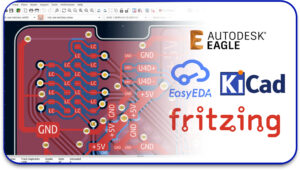
Step 1: Plan Your Circuit
Before laying out your PCB, draw a circuit diagram (also called a schematic). This shows how each part connects. You can use free tools like:
- EasyEDA
- KiCad
- Fritzing
- Autodesk Eagle
Keep your diagram clear. Label each part. Group related items together. This helps later during layout.
Tip: If you’re not sure how to design a PCB circuit board, start small. Try blinking an LED with a switch. Once that works, move to bigger ideas.
Step 2: Choose the Right PCB Type
Not all PCBs are the same. There are many types depending on your needs:
- Rigid PCBs: Hard and fixed shape
- Flexible PCBs: Bendable and thin
- Rigid-Flex PCBs: A mix of both
If your device bends or wraps around something (like a smartwatch), flexible PCB fabrication is a good option. For most home projects, rigid PCBs are enough.
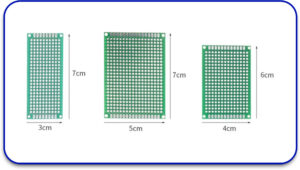
Step 3: Pick Your Board Size and Shape
Decide how big your board should be. Think about:
- The size of your enclosure or case
- Where will each part sit
- Where wires will connect
Don’t make it too tight. Leave space around parts so heat can escape. This also makes soldering easier later.
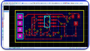
Step 4: Place the Parts (Component Placement)
Now, start your PCB board design. This step is called component placement. It means dragging each part onto the board in your layout tool.
Here’s how to place parts the smart way:
- Put power parts (like batteries or voltage regulators) near the edge
- Keep related parts close together (e.g., a sensor and its chip)
- Don’t overlap parts
- Leave space for holes if you need to screw the board into something.
Think of your board like a puzzle. Each part has its place.
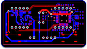
Step 5: Route the Traces
Next, connect all the parts using traces. These are tiny roads that carry electricity.
Here are some tips for good circuit board layout design:
- Keep traces short and direct
- Don’t cross other traces unless on a different layer.
- Use wider traces for power lines.
- Avoid sharp corners (use 45-degree angles instead)
- Keep signal and power traces separate if possible.
Use copper pour for ground connections to reduce noise.
If you’re stuck, most PCB tools have auto-router features. These aren’t perfect, but they help as a starting point.
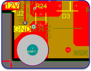
Step 6: Add Labels and Mounting Holes
A finished PCB layout should include the following:
- Labels for each part (like R1, C3, U2)
- Clear pin markers (so you know which way to plug things in)
- Mounting holes if the board needs to attach to a case
This step is small but essential. It helps you debug problems later.
Step 7: Run a Design Rule Check (DRC)
All layout tools include a DRC (Design Rule Check). It finds problems like:
- Traces that are too close
- Missing connections
- Holes placed on traces
Run this before you send your board for production. Fix any warnings or errors.
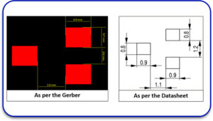
Step 8: Export Gerber Files
Once your layout is done, you need to export Gerber files. These are the standard files used in Custom PCB manufacturing.
They include:
- Copper layers
- Drill layers
- Silkscreen (text)
- Solder mask
Double-check these files using a Gerber viewer before sending them to a PCB manufacturing company.
Step 9: Choose a PCB Manufacturer
Now, it’s time to build your board. Many Custom PCB manufacturing services accept online orders. Some popular ones are:
- JLCPCB
- OSH Park
- PCBWay
- Advanced Circuits (USA)
If you’re in the U.S., look for PCB production USA options for faster shipping. Some companies even offer same-week turnaround.
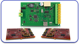
Step 10: Assemble Your Board
After your board arrives, it’s time for assembly. This means:
- Placing each part
- Soldering it in place
- Testing the final circuit
You can do this at home with a soldering iron or hot air gun. For complex builds, use assembly services or kits.
Bonus: Tips for Better PCB Board Layout Design
Here are some quick tips to improve your design:
- Use grids: Keep part spacing even
- Group by function: Power, logic, sensors, etc.
- Plan for expansion: Add extra holes or headers for future parts
- Watch current paths: Keep ground returns short and direct.
- Double-check orientation: Make sure diodes and chips face the right way.
Good PCB board layout design doesn’t happen by accident. It takes time, testing, and learning from mistakes.
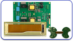
When to Consider Flexible PCB Fabrication
Not all boards are flat and square. If your device:
- Folds
- Bends
- Moves during use
Then, flexible PCB fabrication might be the better option. These boards use flexible plastic material. You see them in cameras, hearing aids, phones, and foldable gadgets.
They cost more but save space and improve reliability in moving parts.
Learning How to Design a PCB Circuit Board
You don’t need to be an engineer to learn how to design a PCB circuit board. Start with small projects. Follow online tutorials. Ask for help in maker forums. And always test before sending a design to production.
With practice, your PCB board designing skills will grow.
Conclusion
A well-designed PCB is the heart of any working device. From the first sketch to the final solder joint, every step counts.
Now that you know the basics of PCB board layout design, you can take your ideas and turn them into working electronics. Whether it’s a hobby project or the start of something big, a good layout leads to great results.
Take your time. Plan carefully. And always think about how the current will flow through your design.
Your next great device starts with a well-laid-out board.


