If you’re working on a product that bends, twists, or folds, a standard PCB might not be enough. That’s where flexible PCB fabrication comes in. Flex PCBs are used in everything from smartphones to medical devices. They let you design compact, lightweight, and durable electronics that still perform under movement. But designing a flexible PCB takes a different approach than a rigid one. This blog will discuss how to design flexible PCBs, what to watch out for, and how to avoid the most common mistakes.
What Is a Flex PCB?
A flex PCB is a thin circuit board made with flexible materials like polyimide. It can bend and twist without breaking, making it perfect for devices with moving parts or limited space.
Flex PCBs can:
- Reduce wiring
- Save space
- Cut down on weight
- Improve reliability in harsh environments.
If you’re building modern electronics, learning flexible PCB design guidelines is a must.
Why Flex Design Needs Special Attention
Flex PCBs may look like standard boards, but they behave very differently. When you bend a board, stress builds up in the copper and material layers. If the design isn’t right, cracks and failures happen fast.
That’s why proper design is just as important as the right materials. Whether you’re working with a PCB manufacturer or a PCB manufacturing company, starting with good design saves you money, time, and frustration later.
Start With a Good Flex Drawing
Before you even begin routing your board, create a flex drawing. This document explains everything the manufacturer needs to know:
- Board dimensions
- Bending zones
- Stiffener areas
- Connector locations
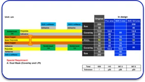
- Stack-up details
A complete and accurate flex drawing prevents misunderstandings. It also helps your PCB manufacturer plan production the right way.
Know Your Flex PCB Thickness Options
One of the most important things to choose is the flex PCB thickness. Thickness affects how much your board can bend, how durable it is, and how it fits into your device.
Common thickness ranges:
| Layer Count | Typical Thickness |
| 1-Layer | 0.1 mm to 0.2 mm |
| 2-Layer | 0.15 mm to 0.25 mm |
| 4-Layer | 0.3 mm and up |
TThinner boards bend more easily but are more fragile. Thicker boards are stronger but stiffer. Talk to your PCB manufacturing company about the right balance for your project.
Key Guidelines to Design Flexible PCBs
Here are simple, straightforward rules you should always follow when designing a flexible PCB:
1. Keep Traces Straight in Bend Areas
Avoid routing traces in zig-zag patterns or at sharp angles in areas that will bend. Curved traces handle bending stress better than sharp corners. Use rounded corners wherever possible.
2. No Vias in Bending Zones
Vias are weak points. If you place them in a bend area, they’ll likely crack over time. Keep all vias in static (non-bending) zones of your board.
3. Use Wider Traces and Spacing
Wider traces lower the chance of cracking. Try to use the widest trace possible based on your space and signal requirements. Also, give each trace more space to reduce stress during bending.
4. Avoid 90° Corners
In flex design, sharp corners are bad. They collect stress, which leads to cracks. Use 45° angles or curves instead.
5. Choose Stiffeners Wisely
A stiffener is a non-flexible material added to parts of your board to support connectors or other components. You must add them in areas where:
- You have a heavy connector.
- The board is soldered.
- Mechanical stress is high.
Make sure your flex drawing marks these areas clearly.
Material Selection Matters
Materials play a significant role in flexible PCB fabrication. The wrong material can lead to failure, even with a great design.
Ask your PCB manufacturer about:
- Polyimide films for flexibility and heat resistance
- Adhesiveless base materials for better flexibility
- Stainless steel stiffeners for extra durability
Also, don’t forget about coverlay. It’s the flexible version of solder mask and protects your circuits.
Routing and Layer Guidelines
Routing on a flexible PCB isn’t the same as on a rigid one. You need to plan carefully:
- Keep critical signal lines away from bend zones
- Route power lines in the center of the stack-up to balance stress
- Use hatched ground planes to improve flexibility without losing shielding.
If you’re working on a multi-layer design, make sure your PCB manufacturing company knows how to manage flex PCB thickness correctly across the layers.
Bending Radius Rules
Don’t bend your board too sharply. Use this rule of thumb:
Bending Radius = 10 × Board Thickness
So, if your flex PCB is 0.2 mm thick, your minimum bend radius should be 2 mm.
Following this rule helps avoid cracking and tearing. If your design needs tighter bends, talk to a PCB manufacturer who specializes in flex circuits.
Testing Your Flex Design
After your board is made, it should go through bend testing. This helps catch problems early. Ask your PCB manufacturing company if they offer mechanical fatigue testing for flex circuits.
You can also test by flexing a prototype manually for a few hundred cycles. If it breaks, go back and review your design.
Mistakes to Avoid
Here are some common errors that can ruin your flexible PCB design:
- Skipping the flex drawing
- Using rigid PCB rules on a flex design
- Not labeling bending zones.
- Placing parts in active bending areas
- Choosing a cheap material that can’t handle bending
Avoiding these mistakes keeps your project on track and saves you money in the long run.
Real-Life Example
Let’s say you’re designing a wearable fitness tracker. It wraps around the wrist, so it needs a flex circuit. You design your traces with 90° corners and put vias near the bend zone. After a few uses, the tracker stops working.
You talk to a PCB manufacturing company that shows you how to route curved traces and move the vias. They also suggest a stronger polyimide material and thinner copper. After these changes, your board lasts 10x longer.
This shows how proper design and choosing the right PCB manufacturer can save your project.
Work With the Right Partner
Not every PCB manufacturing company has experience with flexible circuits. Ask these questions before you begin:
- Have you worked with wearable or bendable devices?
- What materials do you use in flexible PCB fabrication?
- Can you help with stack-up and bending radius planning?
A good partner doesn’t just make the board; they help you design it right.
Final Thoughts
Designing a flexible PCB takes planning, patience, and care. You need to follow the proper steps, choose the right materials, and work with the right team.
Here’s a quick recap of what you need to do:
- Create a detailed flex drawing
- Choose the right flex PCB thickness.
- Keep traces curved and wide.
- Avoid vias and components in bending zones.
- Use good materials like polyimide and coverlay
- Follow proper bending radius rules.
- Test your board before full production.
By following these flexible PCB design guidelines, you’ll avoid common issues and build something that works, and keeps working.
And most importantly, choose a PCB manufacturer or PCB manufacturing company that knows flex PCBs inside and out. Their support can make or break your design.

