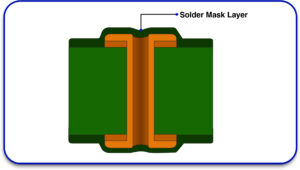
The consideration of the PCB solder mask is critical for the long-term reliability and the performance of the board. The solder mask adds protection against oxidation or corrosion and guarantees accurate soldering during assembly.
Now, consider how the combination of the design of the PCB solder mask alongside high-quality liquid solder mask contributes to the strengthening of the board, decreasing the manufacturer’s burden, and answerinfg the functionality of modern electronics. We, at Blind Buried Circuits, meticulously follow these guidelines to provide high-reliability PCBs for contemporary uses, ranging from aerospace to consumer electronics.
What is a PCB Solder Mask, and Why Use It?
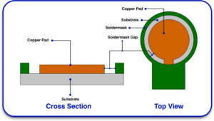
The PCB solder mask features a protective coating placed over the copper traces. Any choice including traditional epoxy coatings, state-of-the-art IPI solder mask, or even newly developed inkjet solder mask technologies must be based on specific application requirements.
In general, application processes and compliance with design standards impact the quality of the solder joint as well as the electrical insulation. Commonly green (although other colors are available), the layer also possesses several key benefits which include:
Prevents solder bridges: Masking prevents unwanted solder flow in between traces which helps mitigate electrical short circuits.
- Protects from corrosion and oxidation: Copper is susceptible to air, water, and moisture, meaning it can be exposed. The mask manages this as an enclosure.
- Improves mechanical durability: The element improves copper’s resilience to physical and environmental stress.
- Provides electrical insulation: The mask guarantees that only predetermined areas are exposed to solder during assembly which gives insulation.
Due to these properties, it is an instrumental part of the design for the masker of PCBs irrespective of the level of intricacy.
4 DFM Guidelines for PCB Solder Mask Design
Compliance with the Design for Manufacturing (DFM) guidelines is crucial upon solder mask design to ensure manufacturability and performance.
1. Via Tenting: Covering vias with the solder mask reduces exposure to shorting which is paramount in modern masker design approaches.
2. Minimum Web Width: To avoid slivers and maintain the structural integrity of green and other colors, a four mil solder mask web and a five mil web respectively should be used.
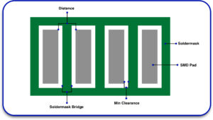
3. Pad-to-Mask Ratio: A one to one (1:1) ratio between the solder mask opening and the underlying pad should be implemented to increase efficiency in alignment and assist in soldering.
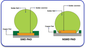
4. SMD vs. NSMD Pads: Solder mask defined (SMD) pads are less effective than non-solder mask defined (NSMD) pads because NSMD pads perform significantly better under stress when liquid solder masks are applied at high densities.
Types of PCB Solder Mask
Understanding the various types of solder masks is key to selecting the right material for your project:-
- Top and Bottom Masks: These refer to solder mask applications on either side of the board, based on component placement and circuit design.Epoxy Liquid Solder Masks: Cost-effective and applied via screen printing, these are ideal for simple boards.
- Liquid Photoimageable (LPI) Solder Masks: Also known as LPI solder masks, these are applied as a liquid and then exposed to UV light for precise patterning. This is the most commonly used method today for advanced PCBs.
- Dry Film Photoimageable Resists: Applied using heat and pressure, these are suitable for high-density and fine-line circuitry but are more expensive.
Each type of PCB solder mask, liquid or dry film, has trade-offs in terms of resolution, cost, and application method..
How is a Solder Mask Applied?
The application of a solder mask involves several meticulous steps, especially when using PCB solder mask techniques:-
1. Cleaning the PCB:-
The PCB is thoroughly cleaned using chemical and mechanical methods to remove dust, oil, and oxidation, which is necessary for proper adhesion.
2. Ink Coating:-
A uniform layer of liquid solder mask is applied over the PCB surface using screen printing, spray, or curtain coating methods.
3. Tack Curing:-
The applied solder mask is partially cured under controlled heat to stabilize it before the imaging process, ensuring dimensional accuracy.
4. Imaging and Exposure:-
A photomask aligned with the board is exposed to UV light, hardening only the areas intended to remain covered.
5. Developing:-
Unexposed, soft solder mask material is removed using a developer solution, leaving openings for pads and vias to receive solder.
6. Final Curing and Cleaning:-
The PCB undergoes full thermal or UV curing to harden the solder mask permanently, followed by cleaning to remove any residue.
This process ensures that only necessary areas are left exposed for soldering, improving the precision of solder mask design.
Solder Mask Processing with Inkjet
Inkjet solder mask application is a rapidly emerging technology in PCB manufacturing that enables the precise, digital deposition of liquid solder mask directly onto circuit boards.
This process removes the need for traditional photo tools used in IPI solder mask methods, significantly streamlining prototyping and small-batch production. By printing only where needed, it minimizes waste and enhances efficiency, offering greater flexibility in solder mask design.
Though still gaining traction in high-volume manufacturing, its potential to improve accuracy and reduce turnaround times makes it a promising option for advanced PCB solder masks’ applications, especially in rapid development and custom designs.
Why choose us?
At Blind Buried Circuits, we are proud to be a leading PCB board manufacturer and turnkey PCB manufacturing and assembly partner, delivering quick-turn and custom solutions to clients across a wide range of industries. With years of experience in PCB production in the USA, our capabilities include advanced Rigid, Flexible, and Semi-Flex circuit manufacturing, all supported by rapid lead times and scalable production volumes—from prototypes to high-volume orders.
As an ISO 9001, ISO 13485, ISO 14001, and IPC-certified EMS provider, we strictly follow QMS and IPC Class 2, 3, and 3A standards. Whether you’re in telecom, IoT, automotive, aerospace, medical, or industrial sectors, Blind Buried Circuits offers reliable, end-to-end PCB solutions tailored to your needs. Trust us to simplify your product development journey with precision, speed, and unmatched quality.
Conclusion
From preventing oxidation and corrosion to ensuring precise soldering during assembly, the PCB solder masks design is essential for achieving long-term board reliability and performance. Whether opting for traditional epoxy coatings, advanced IPI solder mask solutions, or exploring modern inkjet solder mask technologies, selecting the appropriate type based on your application is critical.
Proper application techniques and adherence to design standards directly affect solder joint quality and electrical insulation. A deep understanding of solder mask design, combined with the use of premium liquid solder mask, enhances the board’s durability, reduces manufacturing defects, and ensures high functionality in today’s complex electronics.


