The elevation in the global need for compact and high-functionality electronics has made High-Density Interconnect (HDI) PCBs a prerequisite in contemporary designs. These advanced boards have made it feasible for engineers to integrate higher functionality into smartphones, IoT devices, and even aerospace technologies.
For effective interaction with any reliable PCB manufacturer, knowing the HDI PCB standards and PCB design principles is essential for achieving dependable, high-performance outcomes.
What Makes HDI PCBs Unique?
These PCBs have the industry’s highest wiring density and multiple layers of integrated advanced features, including micro vias, blind vias, and buried vias. They are extensively used in lightweight and compact designs that do not compromise performance.
PCB design and manufacturing standards are the key to such extensive success. Best practices transform functionality, reliability, and manufacturability into reality, even in high-demand environments.
Essential HDI PCB Standards
HDI board performance and quality, compared to industry standards, depend heavily on the procedures used in the PCB design and manufacturing process. These are some of the most integral benchmarks and standards that effective PCB manufacturers are known to observe.
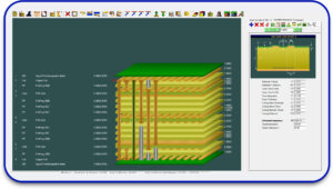
IPC Regulation for HDI PCBs
- IPC-6012D: This rule covers the scope of work and other qualifications for performing rigid printed circuit boards, including HDI-type ones.
- IPC-2226: This concentrates on HDI topologies, including instruction for apparatus design with high wiring density, with an emphasis on plan layout.
Following the IPC standards allows designers and fabricators of HDI-embedded PCBs to ensure that the PCBs can sustain the complex application’s mechanical, thermal, and electrical needs.
Learn About: IPC and UL Standards for Next-Gen MedTech PCB Designs
UL Accreditation
UL 796 certification is a must for safety and reliability on HDI PCBs. It certifies that adequate materials and construction processes are produced under stringent fire and safety requirements.
ISO Norms
For the medical, aerospace, and automotive industries, quality management procedures using ISO 9001 and ISO 13485 must be designed and observed during PCB design and manufacturing processes.
Recommendations for HDI PCB Development
The full benefits of HDI PCB technology can be attained by addressing the best practices of these boards, which have unique features and the latest design challenges, over other standard components.
1.Optimized Layer Structure
To achieve miniaturization of PCB size, the integrity of signals can be appended using a combination of stacked, staggered, and skip vias. The design should use stacked vias for maximum area efficiency.
2. Via Technologies
These new via designs improve component density because they offer signal routing flexibility and lessen signal loss or interference.
3. Material Selection
The chosen materials for the component must have low dielectric constants, excellent thermodynamic properties, and the ability to endure high-frequency operation alongside extremely harsh environments.
4. Signal Integrity Examination
Outline trace widths, space, and impedance to lessen the chance for loss signals and electromagnetic interference (EMI). A well-managed signal’s integrity guarantees the effectiveness of high-frequency applications.
5. DFM
Involve a PCB manufacturer with sufficient industry experience in the design process to account for manufacturability. If considered in the design phase, DFM will decrease time and reduce errors made in production.
Problems for HDI PCB Manufacturing
HDI PCB manufacturing does have obstacles. Suppliers need to accomplish many steps, from accurately drilling to integrating complex laminations, to achieve optimal success.
1. Microvia Drilling
The laser needs to be engaged to provide high accuracy through precise control when producing tiny microvias.
2. Registration accuracy
Layer alignment plays a crucial role with stacked vias in HDI boards requiring accurate registration.
3. Thermal Management
Overheating can cause serious problems for the device and can be resolved through the right materials accompanied by sound thermal management strategies for HDI PCBs.
4. Cost Considerations
The “High-Density Interconnect” or HDI technology constructed with a PCB layer requires time and effort, which tends to incur many expenses. Selecting the proper PCB manufacturing partner helps minimize expenditures while ensuring quality.
Advantages of HDI PCBs
Just like traditional PCBs, HDI PCBs have their advantages, too, and they extend across different industries. Some of them are as follows:
- Enhanced Performance: Faster transmission and improved signal-to-noise ratio.
- Compact Designs: Smaller boards that are slimmer and lighter.
- Increased Functionality: More components packed within a small area.
- Improved Reliability: Guarantees low interference and noise.
Applications of HDI PCBs
HDI PCBs have a wide usage range in many sectors, for example:
- Consumer Electronics: Smartphones, tablets, and wearables.
- Automotive: Advanced driver assistance systems (ADAS) and infotainment.
- Medical Devices: Compact imaging systems and diagnostic equipment.
- Aerospace and Defense: Communication and navigation high reliability systems.
- IoT Devices: Smart homes and industrial automation.
Partnering with the Right PCB Manufacturer
In any business dealing with HDI PCB, you must not lose sight of your choice of PCB manufacturers as it is a critical risk factor. Look for a partner who offers:
- Expertise in HDI PCB Manufacturing: Having sufficient resources and capabilities is a prerequisite.
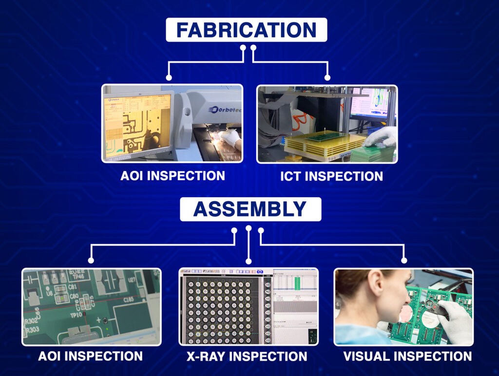
- Comprehensive Quality Control: Compliance with IPC, UL, and ISO requirements.
- Customer Support: Regularly helps you during the PCB design and production stage.
- Advanced Technologies: Modern equipment that guarantees accuracy in manufacture.
It is of utmost importance to analyze certain standards and design procedures in parallel with HDI PCB manufacturing, which continues to change with innovation in new businesses. Engaging in business with a reputed PCB manufacturer guarantees that the PCB designs provided meet the goals set regarding quality, reliability, and performance.
No matter if you are working on a new product or an existing one, expert advice always plays an important role in achieving success. Contact Blind Buried Circuits so that we may assist you in achieving your goals through tailored HDI PCBs designed specifically for your business needs.

