High-Density Interconnect (HDI) PCBs are at the heart of modern electronics. From smartphones to aerospace systems, they enable compact, high-performance designs. However, designing and manufacturing HDI boards is not simple. You need to balance HDI manufacturability with HDI PCB cost to get the best results.
If you’re working with a PCB board manufacturer, making the right choices early in the design phase can help you save money while ensuring a reliable board. In this guide, we’ll break down the key considerations for custom PCB production, helping you understand the trade-offs between cost and manufacturability.
What Makes HDI Boards Different?
An HDI PCB is designed with higher wiring density per unit area than traditional PCBs. It uses microvias, blind vias, buried vias, and fine traces to connect components efficiently. This allows for smaller form factors and better electrical performance.
Why Choose HDI Boards?
- Miniaturization – Smaller boards mean smaller devices.
- Better Performance – Shorter paths reduce signal loss and interference.
- Increased Reliability – Microvias offer better durability than traditional through-hole vias.
- Fewer Layers Needed – With high-density routing, you can achieve the same functionality with fewer layers, reducing thickness.
However, achieving these benefits requires precision manufacturing, which affects both cost and design choices.
Key Factors Affecting HDI Manufacturability
Manufacturing HDI boards involves advanced techniques that must be carefully planned to avoid unnecessary costs. Here are some key factors that impact manufacturability:
1. Layer Stack-Up and Material Choice
Your layer stack-up affects both cost and manufacturability. The more layers you use, the more expensive the board becomes. Choosing the right materials is also critical.
- High-Tg materials (like polyimide and ceramic-filled laminates) offer better thermal performance but add cost.
- Standard FR-4 can be used in lower-layer HDI designs to keep costs down.
- Copper thickness must be optimized to ensure good conductivity without adding excess weight.
A well-balanced stack-up ensures manufacturability while keeping costs in check.
2. Via Structures and Drilling Complexity
Microvias, blind vias, and buried vias are essential for HDI PCB design, but they affect manufacturing complexity:
- Stacked microvias provide high performance but require multiple laminations, increasing cost.
- Staggered microvias are easier to manufacture and reduce cost.
- Via-in-pad designs improve signal integrity but require extra processing, such as via filling and capping.
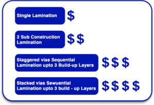
The fewer the sequential lamination steps, the lower your manufacturing costs will be.
3. Trace Width, Spacing, and Aspect Ratio
With HDI, you need finer traces and smaller spacing to fit everything on a compact board. But this increases fabrication difficulty:
- Ultra-fine traces require more precise etching, adding to production costs.
- Aspect ratio limitations must be considered to prevent manufacturing defects.
- Controlled impedance is crucial for signal integrity in high-speed applications.
Working with an expert PCB board manufacturer ensures your design meets the necessary tolerances.
4. Drilling and Registration Tolerances
Laser drilling is required for HDI manufacturability, but it has challenges:
- Tight tolerances mean that misalignment can lead to defects.
- Multiple lamination cycles increase processing time and cost.
- Registration accuracy is critical to avoid open circuits.
Proper design planning minimizes these risks, reducing scrap rates and improving yield.
Cost Considerations in HDI PCB Manufacturing
While HDI PCBs offer many benefits, their manufacturing cost can be high if not managed properly. Here’s what drives costs and how to reduce them:
1. Number of Sequential Laminations
Each additional lamination cycle adds cost. You can lower costs by:
- Use staggered vias instead of stacked vias when possible.
- Minimizing sequential laminations to keep manufacturing steps efficient.
- Collaborating with your PCB board manufacturer to optimize stack-up design.
2. Material Costs
HDI boards often require high-performance materials, which can be expensive:
- Low-loss dielectric materials improve signal integrity but raise costs.
- Copper foil thickness impacts conductivity and pricing.
- Choosing the right substrate can significantly lower manufacturing expenses.
Work with a custom PCB production expert to find cost-effective material options.
3. Manufacturing Yield and Scrap Rates
The tighter the design tolerances, the higher the risk of manufacturing defects. Defects lead to scrap, which increases costs. Reduce waste by:
- Optimizing for Design for Manufacturability (DFM).
- Avoiding unnecessary ultra-fine features that increase complexity.
- Partnering with an experienced PCB manufacturer to ensure precision.
4. Via Drilling and Filling
Via-in-pad, filled vias, and plated-over vias add to production costs. Reducing the number of these special vias lowers overall pricing.
5. Testing and Quality Assurance
Electrical testing and reliability checks add cost but ensure PCB durability. Some ways to keep costs reasonable:
- Use Automated Optical Inspection (AOI) to catch defects early.
- Perform electrical tests selectively rather than on every board.
- Choose a trusted manufacturer with a track record of high-yield production.
How to Balance Manufacturability and Cost in HDI PCB Design
You can make smart choices that reduce costs while maintaining manufacturability. Here’s how:
1. Work With an Experienced PCB Manufacturer
A skilled PCB board manufacturer provides:
- Expert design reviews to optimize for manufacturability.
- Cost-effective material recommendations.
- Precision fabrication techniques that improve yield.
2. Optimize Your Stack-Up Early
Fewer layers = lower cost. To optimize:
- Choose materials that balance cost and performance.
- Plan via placement strategically to reduce drilling complexity.
- Use standard dielectric thicknesses to improve manufacturability.
3. Reduce Unnecessary Features
Not every HDI PCB needs the most advanced features. Ask yourself:
- Do I really need ultra-fine traces?
- Can I reduce via complexity without sacrificing performance?
- Is via-in-pad necessary, or can I use regular vias?
Small adjustments can cut costs significantly.
4. Use Design for Manufacturability (DFM) Guidelines
A DFM-friendly design:
- Reduces unnecessary drilling steps.
- Uses standard material thicknesses.
- Avoids excessive microvias and fine-pitch features.
Balancing HDI manufacturability and HDI PCB cost requires careful planning. While HDI boards improve performance and miniaturization, unnecessary complexity can drive up expenses. By choosing the right stack-up via structures, materials, and manufacturing partners, you can achieve cost-effective custom PCB production without compromising quality.
At Blind Buried Circuits, we specialize in HDI PCB design and manufacturing, providing cost-effective, high-performance solutions tailored to your needs. Need expert guidance? Contact us today to optimize your HDI PCB project!


