Every PCB design begins with a schematic diagram, which is a visual representation of the components, their contacts, and the electronic circuit’s functionalities. Accurate and clear schematics allow engineers to produce custom PCBs and manufacture them without errors. The challenge lies in designing accurate, functional, and precise board schematics that minimize the primary issues encountered during PCB production.This article will help you understand PCB schematics, teach you how to create them, and provide tips for modifying PCB circuit diagrams so that they work better.
How to Make an Effective Schematic Diagram of PCB Design
As the name suggests, a schematic diagram of a PCB visually describes how the electronic components of the PCB relate to one another and how they will operate. It serves as a guide for designers and PCB fabricators to help them devise, diagnose, and put together unique projects in PCB production.
Independent of the tools used to design the schematic diagram, it needs to have proper details of all components necessary to make the PCB diagram function correctly. So, why is a schematic needed for PCB design?
A Two-Layer Procedure for Schematic Diagram of PCB Design Can Be Created Using the Following
1. The logical structure of the schematic affects the order of operations in a schematic.
- Before progressing to laying out the physical PCB, a schematic serves as a circuit representation that encompasses all the fragments.
2. Schematic diagrams for PCBs can be considered multifunctional devices because they help reveal a feasible arrangement.
- A well-structured schematic aids engineers by enabling them to spot errors before the construction of the model.
- Schematic errors can result in short circuits, the wrong connections, or even component damage.
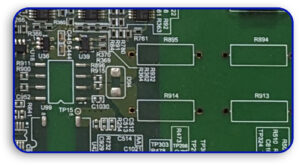
3. Helps with PCB Manufacturing and Assembly
- A precise schematic assists companies that manufacture PCBs in assembling the board accurately.
- It ensures that all the components are placed properly and the soldering is done. It also allows the signals to propagate through the PCB as intended.
4. Enhances Performance and Signal Integrity
- A well-thought-out and implemented schematic reduces parasitic effects while increasing the PCB’s signal integrity.
- Distributing power and grounding properly eliminates the chances of noise or interference.
Step by Step Instructions to Draw a PCB Schematic Diagram
Follow these instructions to achieve a professionally looking and efficiently working PCB schematic.
1. Determine Circuit Specifications

Firstly, you need to know the purpose of the circuit, its required power, and expected performance.
1.1 Functionality Breakdown
- What problem does this circuit solve?
- Is the circuit a power supply device, sensor, communication module, or microcontroller-based device?
1.2 Voltage and Amperage Breakdown
- Determine operating voltage levels. 3.3, 5, and 12 are typical voltages.
- Choose traces and components for the PCB based on the power requirements.
1.3 Determine Inputs And Outputs Signals
- Signals can be of many types, analog or digital, high-speed or low power.
- Evaluate the risk of interference or noise.
2. Select the Appropriate PCB Layout Software
Professional software helps in placing components, making net connections, and checking the design more efficiently.

2.1 Suggested Tools for PCB Schematics Altium Designer allows for advanced levels of complexity when creating PCB layouts.
KiCad – It is an open-source software and much preferred for personalized created PCB’s
Eagle CAD – Famous among small businesses and DIY’ers.
OrCAD – A preference for professional quality schematic designs of PCB boards.
3. Create A New Schematic Project
After selecting the design tool, here are the steps to follow.
3.1 Workspace Configuration
- Set the page format, grid dimensions, and page rotation as needed.
- Select device libraries for quick associations.
3.2 Simplify Circuit Design Work
- Separate functional parts(e.g., Power, signals, microcontroller, sensors) logically.
- In the case of more complicated circuits, use diagrams in blocks.
4. Include Components and Their Corresponding Symbol
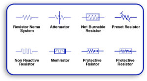
A PCB schematic diagram includes various electronic elements, including resistors, capacitors, ICs, and transistors.
4.1 Picking Components Out of The Library’s Compilation.
- Take the components from the software’s available component library.
- Make sure the symbol and footprint are components that do exist in real life.
4.2 Logical Component Positioning.
- Position components in an orderly manner without distancing associated elements too far apart.
- Adhere to best practices throughout the industry.
5. Make Electrical Connections
It would guarantee that the power and signal circuits are properly connected to the circuit.
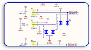
5.1 Correctly Using Nets and Wires
- Provide interconnections among members using named nets instead of crossed wires.
- Utilizing various colors for power, ground, and signals for easy identification.
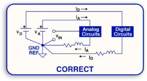
5.2 Giving Power and Ground References
- Make sure that VCC, GND, and power rails are identifiable and visible.
- The aim of avoiding the long floating power lines that cause interference is described in detail above.
6. Label Components Clearly
The label makes sure that the schematic is straightforward to read through and troubleshoot.
6.1 Assign Reference Designators
- Assign values for R1, C1, or U1 to resistors, capacitors, and ICs.
- Make sure the designators are the same throughout the schematic.
6.2 Add Notes and Annotations
- Record the values and ratings for components.
- Make comments to note vital information to avoid misunderstanding and assist in troubleshooting.
7. Verify Signal Flow and Connectivity
Electrical Rule Check (ERC) runs to troubleshoot a design-based issue.
7.1 Checking for Errors
- Check for connections that appear to be missing, pins that are not connected, and signals that have short circuits.
- Resolve all warnings or errors issued by the design tools.
7.2 Performing Design Rule Check (DRC)
- Confirm there is compliance with the guidelines set by the ordering.
- Calculating footprint metrics ensures there is no overreach with the components by confirming spacing between traces and widths.
Learn About: Common Errors in PCB Design That Lead to Assembly Failures
Additional Recommendations For Enhancing PCB Design Schematic
1- Logical Layout Design Restrictions
1.1 Group Components by Function
- Organize the power supply signal UPs and noise reductions as individual circuits.
- For thoroughly detailed and more intricate projects, hierarchical designs should be applied.
1.2 Avoid Unnecessary Crossings
- Adopting named nets instead of an intricate web of wires reduces the need to label each component.
- Remove as many intersections as possible, as they tend to clutter the overall appearance.
2. Foster Better Grounding And Power Distribution
2.1 Implement Proper Grounding
- A single plane devoid of noise, leading to the dedicated ground, should be used.
- Prevent any sort of interference stemming from loops of ground.
2.2 Applying Decoupling Capacitors
- Add capacitors next to integrated circuits (ICs) for effective voltage regulation.
- Choose a capacitance that matches the desired noise voltage level.
3- Before Doing the PCB Layout
3.1 Check Values of All Components in the PCB
- Check if the components’ values fit the specifications of the design.
- Check the tolerances for capacitors and resistors.
3.2 Make Sure ERC & DRC Are Run Final.
- Close the remaining error or warning messages.
- Ensure correctness in connections before proceeding with the layout.
Custom PCB design starts with a schematic that ultimately defines the performance a PCB can achieve in terms of its intended application, reliability, and manufacturability. With a proper guidelines framework, it is possible to generate schematics without errors to facilitate the PCB layout and fabrication. To benefit from the industry’s standards for custom PCBs, it is necessary to work with a proficient custom PCB manufacturer to guarantee that the design is of the highest optimized quality. A well-structured schematic serves as a recipe for any PCB, novice or veteran, regardless of the design’s complexity, whether single-board or multi-layer.


I’ve read a few good stuff here. Certainly worth bookmarking for revisiting. I surprise how much effort you put to create such a magnificent informative website.