When designing PCBs for aerospace, medical, and high-reliability electronics, have you ever faced performance issues due to contamination or material failure? One often overlooked problem in PCB board assembly manufacturing is PCB outgassing—the release of trapped gases from PCB materials under vacuum or high-temperature conditions.
Outgassing can cause major failures, such as:
- Circuit malfunctions due to trapped gases forming conductive paths.
- Adhesion failures in coatings and solder joints.
- Optical and mechanical issues in space and medical applications.
To prevent these issues, it’s essential to focus on mitigating outgassing in PCBs through proper PCB material selection, optimized manufacturing processes, and careful design considerations.
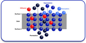
What is PCB Outgassing?
PCB outgassing is the release of volatile gases from PCB materials when exposed to heat, vacuum, or low-pressure environments. These gases can lead to:
- Formation of voids in solder joints.
- Contamination of sensitive electronic components.
- Breakdown of insulation resistance.
Industries most affected by PCB outgassing:
- Aerospace & Satellites: Outgassing can create a film of contaminants that blocks sensors and optics, impacting performance.
- Medical Devices: Trapped gases in PCBs can interfere with sterilization and affect device reliability.
- Military & Defense: Outgassing in critical electronic components can compromise system functionality in harsh environments.
- Automotive & Industrial Electronics: High temperatures inside automotive control units can cause PCB materials to degrade faster.
How Does Outgassing Affect PCB Performance?
1. Reduced Electrical Reliability
Outgassing releases gases that can form conductive paths, leading to short circuits and signal integrity issues. This is especially concerning in high-frequency and high-voltage PCBs.
2. Solder Joint and Coating Defects
Gas bubbles trapped inside solder joints can cause:
- Weak solder bonds, leading to premature failure.
- Poor adhesion of conformal coatings, reducing protection.
3. Optical Contamination in Space Applications
In vacuum conditions, PCB outgassing can release molecular contamination that settles on optical lenses, sensors, and imaging devices, severely affecting performance.
4. Thermal Stress and Component Failure
Trapped gases expand when heated, causing:
- Micro-cracks in PCB layers.
- Delamination and warping of PCB materials.
For high-temperature applications, choosing the right materials and manufacturing techniques is crucial for minimizing outgassing.
Key Strategies for Mitigating Outgassing in PCBs
To prevent outgassing effects on electronics, follow these best practices during PCB manufacturing assembly:
1. Choose Low-Outgassing PCB Materials
Selecting low-outgassing laminates, prepregs, and substrates is the first step in reducing gas release.
Recommended materials for low-outgassing PCBs:
- Polyimide-based substrates – Ideal for high-temperature applications.
- PTFE (Teflon) laminates – Used in high-frequency PCBs.
- Ceramic-filled laminates – Provide excellent thermal stability.
Avoid materials with high volatile content, such as standard FR-4, unless modified with additional processing.
2. Optimize PCB Layer Stack-Up
Proper PCB design can help minimize outgassing risks by:
- Reducing the number of high-resin layers (resins tend to trap gases).
- Using thinner dielectric layers to reduce gas formation.
- Adding venting structures to allow gases to escape before encapsulation.
3. Pre-Baking PCB Materials Before Assembly
A pre-bake process removes moisture and trapped gases before components are soldered onto the PCB.
Standard pre-baking process:
- Bake PCBs at 125°C to 150°C for 6–24 hours (varies based on materials).
- Use a vacuum bake process for even better gas removal.
This significantly reduces voiding in solder joints and prevents future gas release.
4. Use High-Purity Solder and Flux
Low-quality flux and solder can contain volatile compounds that increase outgassing risks. To prevent contamination:
- Use no-clean flux or low-residue flux.
- Choose high-purity solder with minimal impurities.
- Avoid water-soluble fluxes that may trap moisture.
5. Apply Controlled Curing of PCB Coatings and Adhesives
Improper curing of conformal coatings, adhesives, and potting compounds can trap volatiles, leading to outgassing failures.
To avoid this:
- Cure coatings slowly at manufacturer-recommended temperatures.
- Use vacuum curing for aerospace and medical-grade PCBs.
- Choose low-VOC (Volatile Organic Compound) adhesives for better reliability.
6. Use Venting Paths for Trapped Gases
Designing venting paths in PCB layouts helps gases escape before they cause defects.
Best practices include:
- Adding via holes near solder pads to allow trapped gas to exit.
- Avoiding closed cavities in multilayer PCBs.
- Incorporating thermal relief pads to reduce gas buildup in high-power circuits.
7. Perform Advanced Testing for Outgassing Control
Testing ensures that the PCB meets low-outgassing requirements before deployment.
Common outgassing tests include:
- Total Mass Loss (TML) and Collected Volatile Condensable Materials (CVCM) testing – Required for aerospace and space-grade PCBs.
- Thermogravimetric Analysis (TGA) – Measures material degradation under heat.
- Fourier Transform Infrared Spectroscopy (FTIR) – Detects residual volatiles in PCB coatings.
Industry Standards for Low-Outgassing PCBs
Many industries require PCBs to meet strict outgassing standards. Some important guidelines include:
- NASA ASTM E595 – Used for space and satellite PCBs.
- IPC-4101 – Specifies requirements for PCB laminate materials.
- MIL-STD-883 – Military standard for electronic components.
- ISO 14644-1 – Defines cleanroom standards for contamination-sensitive applications.
If your PCB design needs to comply with aerospace, medical, or defense requirements, always verify low-outgassing materials and manufacturing processes.
How Blind Buried Circuits Ensures Low-Outgassing PCBs
At Blind Buried Circuits, we specialize in PCB board assembly manufacturing with strict contamination control to minimize outgassing risks. Our turnkey PCB manufacturing approach includes:
- Low-Outgassing Material Selection: We source NASA-approved laminates and high-purity solder materials.
- Advanced Pre-Baking & Vacuum Processing: Our thermal and vacuum treatments remove trapped gases before assembly.
- Precision PCB Manufacturing Assembly: We use controlled soldering, flux application, and conformal coating processes to reduce volatile release.
- Comprehensive Testing & Compliance: We meet IPC, MIL, and NASA standards for outgassing control in PCBs.
Need reliable low-outgassing PCBs for critical applications? Contact us today to discuss your project requirements!
Final Thoughts
Outgassing effects on electronics can lead to circuit failures, contamination, and reduced PCB lifespan. To prevent these issues, PCB manufacturing assembly should focus on:
- Using low-outgassing materials
- Optimizing PCB design for venting
- Applying pre-baking and controlled curing
- Testing for outgassing control before deployment
For high-reliability PCBs in aerospace, medical, and defense industries, working with an experienced PCB manufacturer ensures the best material selection and manufacturing processes. At Blind Buried Circuits, we guarantee low-outgassing PCB solutions with precision engineering and compliance with industry standards. Let’s build your next PCB with maximum reliability, get in touch today!


