Want to know how your circuit really performs at high frequencies? Then, it’s time to understand S-parameters and how to measure them using a Vector Network Analyzer (VNA). S-parameters (short for scattering parameters) help engineers check how signals behave in a circuit, especially at high speeds. They tell you if your signal is getting reflected, absorbed, or passed along cleanly.
This blog will discuss what S-parameters are, why they matter, and how to measure them using a Vector Network Analyzer. If you’re into RF design, high-speed digital PCBs, or even just testing prototypes from fast PCB manufacturing sources, this skill is essential.
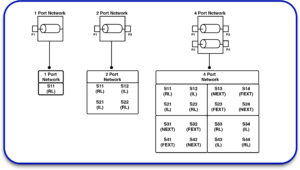
What Are S-Parameters?
S-parameters describe how electrical signals behave when they enter and exit a system. These systems could be anything, cables, filters, antennas, amplifiers, or even a printed circuit board.
Each “S” value represents a behavior:
- S11 – Input reflection (how much signal bounces back at the input)
- S21 – Forward transmission (how much signal goes through the device)
- S12 – Reverse transmission (output back to input)
- S22 – Output reflection
Together, these S parameter measurements tell you if your circuit handles signals correctly or wastes power through reflections.
Why S-Parameter Measurements Matter?
Modern electronics, like 5G, satellites, or even gaming PCs, operate at ultra-high frequencies. At these speeds, signal reflections, interference, or mismatched impedance can ruin performance.
S-parameters let you:
- Diagnose signal integrity issues
- Verify component performance
- Ensure your design matches the PCB manufacturer’s specs.
- Optimize trace layouts in fast PCB manufacturing scenarios.
Engineers working on antennas, RF devices, or high-speed PCBs can’t skip this step.
Learn About: Best EMI and RF Sheilding Methods for Flex PCBs
What Is a Vector Network Analyzer (VNA)?
A Vector Network Analyzer (VNA) is a test tool that measures S-parameters. It sends signals to your device and then records what comes out. It shows:
- How much signal is reflected
- How much passes through
- How phase and magnitude change
Unlike a regular multimeter or oscilloscope, a network analyzer electrical test tool works at high frequencies (from MHz up to many GHz).
How to Perform VNA S Parameter Measurement
Here’s a simple step-by-step guide on how to measure S-parameters using a VNA:
Step 1: Set Up Your Equipment
You’ll need:
- A Vector Network Analyzer (2-port is most common)
- Cables and connectors (with matched impedance)
- Calibration kit (often included with your VNA)
- The DUT (Device Under Test – your PCB or component)
If your PCB comes from a fast PCB manufacturing source, check connector type and layout before testing.
Step 2: Calibrate the VNA
Before taking any measurements, you must calibrate the VNA. This removes the effects of the cables and connectors, so you only measure the DUT.
Use the calibration kit to perform the following:
- Open
- Short
- Load
- Through
This step is critical for accurate S parameter measurements. Most VNAs guide you through it on screen.
Step 3: Connect the Device Under Test (DUT)
After calibration, connect your DUT between the VNA’s ports. Port 1 sends the signal, and Port 2 receives it.
Double-check the connections for:
- Proper contact
- No bent pins or loose connectors
- Consistent impedance (typically 50 ohms)
Using a line pair test tool can help check if your signal and ground paths are clean and reliable.
Step 4: Configure the VNA Test
Set these parameters:
- Frequency range (based on your design or PCB function)
- Power level (start low and increase only if needed)
- Number of points (more points = more detail)
- Sweep type (linear is common, log for wide range)
Now, you’re ready to run a VNA S parameter measurement.
Step 5: Measure and Analyze the Data
Once you start the sweep, the VNA displays your S parameters on-screen as graphs or Smith charts.
Here’s what to look for:
- S11: Should be low (means less signal is reflected)
- S21: Should be high (means most signal passes through)
- S12/S22: Important for 2-way circuits or amplifiers
Watch for sharp dips or spikes; these could mean resonance, impedance mismatch, or faulty solder joints on your PCB board.
Mixed Mode S Parameters – When to Use Them
In high-speed digital systems, you may deal with differential signals (like USB, HDMI, or Ethernet). Here, mixed mode S parameters come in.
These help analyze:
- Mode conversion (from differential to common mode)
- Crosstalk between lines
- Signal integrity in twisted pair layouts
If your project includes differential pairs, mixed-mode analysis is a must.
Real-World Uses in PCB Manufacturing and Design
Many PCB manufacturers now offer boards designed for RF and signal testing. For example, a PCB with coaxial connectors or a breakout board for VNA analysis.
Whether you’re building antennas, sensors, or communication modules, S parameter measurements help you:
- Check board quality from your PCB manufacturing company.
- Validate material choices (FR4, Rogers, etc.)
- Fine-tune layouts for low-return loss
Fast PCB Manufacturing + Signal Testing
When ordering from a fast PCB manufacturing service, make sure to:
- Trace widths and spacings are accurate
- Via placement doesn’t affect signal paths.
- Boards are tested before shipping.
Some advanced fabs offer S parameter test reports as part of QA for high-frequency PCBs.
Bonus Tip: Combine S Parameters with Simulation
Before you even build your board, try simulating S-parameters in tools like:
- Keysight ADS
- Ansys HFSS
- CST Microwave Studio
- KiCad (for fundamental analysis)
This helps catch layout issues early, saving time and money.
What Each S Parameter Tells You
| S-Parameter | What It Shows | Ideal Value |
| S11 | Input reflection | Close to 0 dB |
| S21 | Forward transmission | High as possible |
| S12 | Reverse transmission | Low |
| S22 | Output reflection | Close to 0 dB |
Final Thoughts
Knowing how to measure S parameters using a Vector Network Analyzer opens up a deeper level of control in electronics design. Whether you’re developing RF devices or troubleshooting a high-speed PCB, this skill is worth learning. Use proper tools, calibrate carefully, and work with a reliable PCB manufacturer who supports precision layouts. And remember: every successful signal path starts with the right test method. Need help selecting a VNA or designing a board for high-frequency testing? Reach out today and get expert support from seasoned PCB engineers.


